Low temperature P+ polycrystalline silicon material for non-volatile memory device

a memory device and low temperature technology, applied in the direction of bulk negative resistance effect devices, semiconductor devices, electrical equipment, etc., can solve the problems of dielectric breakdown, other performance degradations or problems that may occur as the device size shrinks, and hinder the operation of the proper device, so as to achieve a wider range of applicability

Active Publication Date: 2014-02-25
INNOSTAR SEMICON SHANGHAI CO LTD
View PDF172 Cites 67 Cited by
  • Summary
  • Abstract
  • Description
  • Claims
  • Application Information

AI Technical Summary

Benefits of technology

[0010]Many benefits can be achieved by ways of the present invention. Embodiment according to the present invention provide a method to form a polycrystalline silicon material having a desirable electrical properties at a deposition temperature of no greater than 450 Degree Celsius, well within a thermal budget to be formed ay in a backend of a CMOS processes. The dopant species (for example, boron species for a p doped) in the polycrystalline silicon material are activated during deposition and does not need an anneal process further simplify the fabrication process and enhance device yield. Additionally, the non-memory device can be fabricated using conventional semiconductor process without modification to the process equipment. Depending on the embodiment, one or more of these benefits can be realized. One skilled in the art would recognize other modifications, variations, and alternatives.

Problems solved by technology

However, as field effect transistors (FETs) approach sizes less than 100 nm, physical problems such as short channel effect begin to hinder proper device operation.
For transistor based memories, such as those commonly known as Flash memories, other performance degradations or problems may occur as device sizes shrink.
With Flash memories, a high voltage is usually required for programming of such memories, however, as device sizes shrink, the high programming voltage can result in dielectric breakdown and other problems.
Similar problems can occur with other types of non-volatile memory devices other than Flash memories.
A common drawback with these memory devices include that they often require new materials that are incompatible with typical CMOS manufacturing.
As another example of this, Fe-RAM and MRAM devices typically require materials using a high temperature anneal step, and thus such devices cannot be normally be incorporated with large volume silicon-based fabrication techniques.
Additional drawbacks with these devices include that such memory cells often lack one or more key attributes required of non-volatile memories.
As an example of this, Fe-RAM and MRAM devices typically have fast switching (e.g. “0” to “1”) characteristics and good programming endurance, however, such memory cells are difficult to scale to small sizes.
In another example of this, for ORAM devices reliability of such memories is often poor.
As yet another example of this, switching of PCRAM devices typically includes Joules heating and undesirably require high power consumption.

Method used


Image

  • Low temperature P+ polycrystalline silicon material for non-volatile memory device
  • Low temperature P+ polycrystalline silicon material for non-volatile memory device
  • Low temperature P+ polycrystalline silicon material for non-volatile memory device

Examples


Embodiment Construction

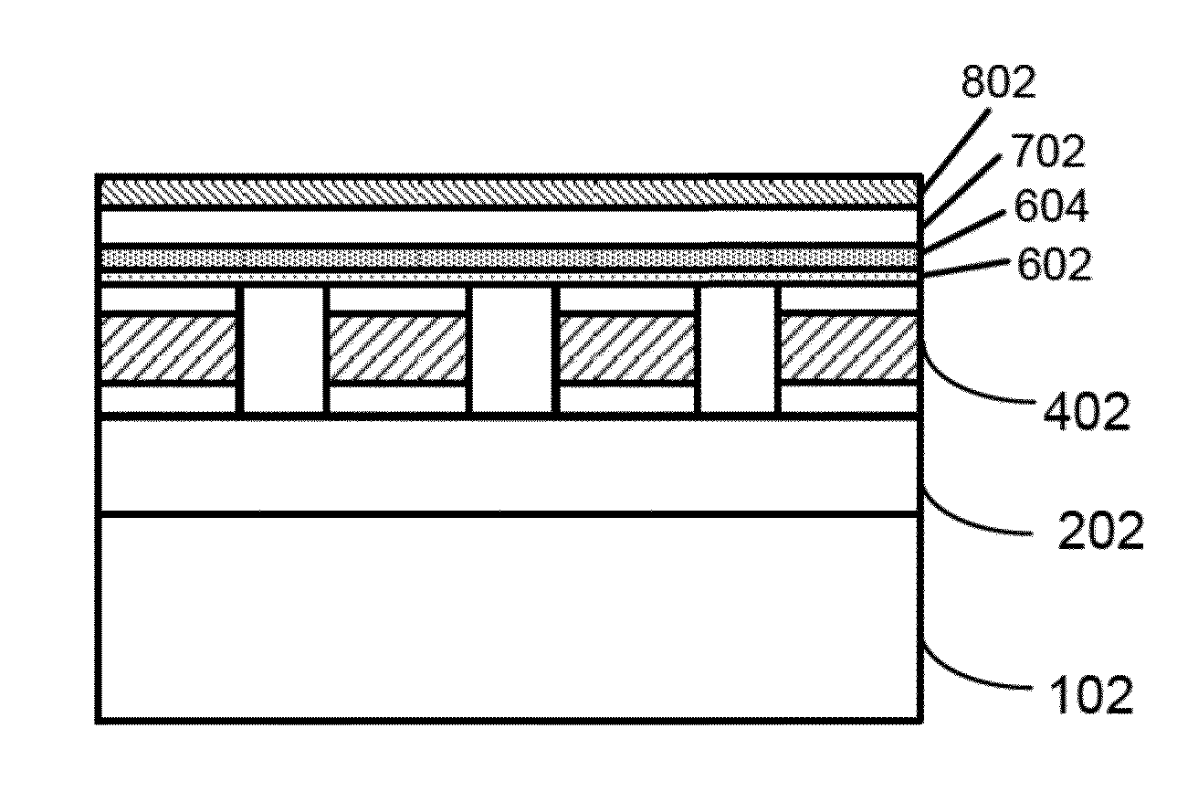
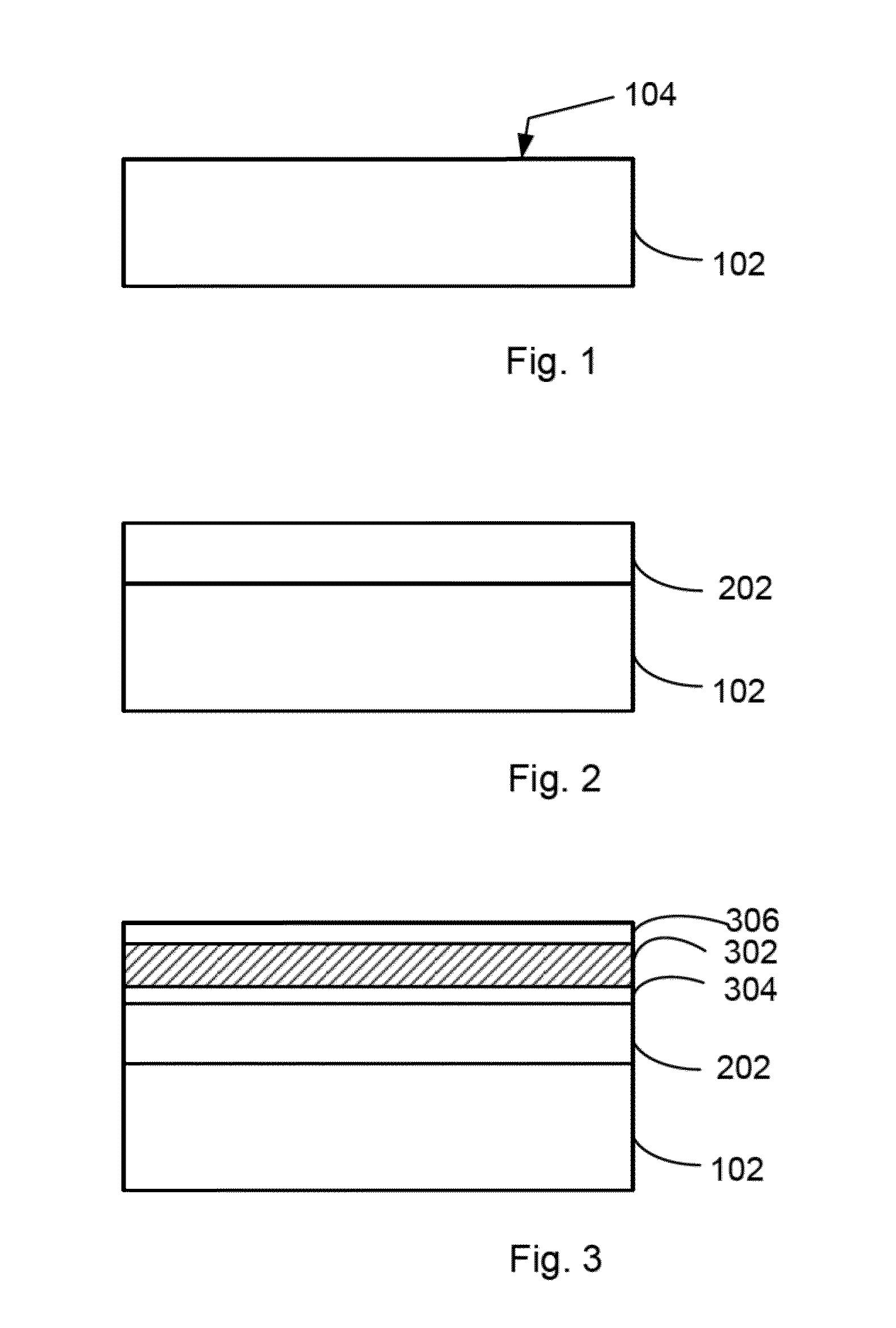
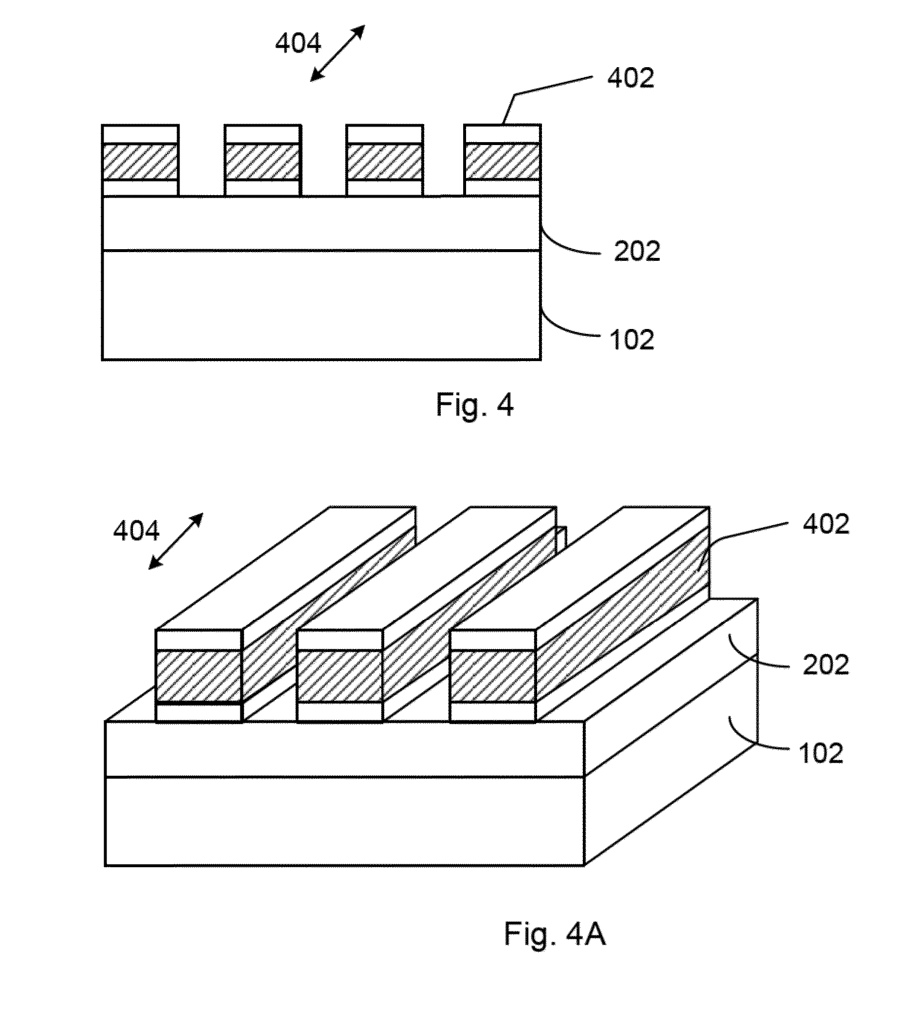
[0017]Embodiments according to the present invention are related to switching devices. More particularly, the present invention provides a structure for resistive switching device and a fabrication method compatible with conventional CMOS processes. Embodiments of the present invention have been applied to a resistive random access memory device, which is non-volatile. But it should be recognized that embodiments according to the present invention can have a much broader range of applicability.

[0018]The terms “Top” or Bottom” are for the purpose of illustration only and should not be construed to be limiting.

[0019]Resistive switching devices usually comprise of a bottom electrode, a top electrode, and a resistive switching material sandwiched between the top electrode and the bottom electrode. Resistive switching devices using amorphous silicon or certain metal oxide, for example, zinc oxide as the resistive switching material require a buffer layer between the resistive switching m...


PUM

PropertyMeasurementUnit
thicknessaaaaaaaaaa
on-state currentaaaaaaaaaa
sizesaaaaaaaaaa

Abstract

A method of forming a non-volatile memory device. The method includes providing a substrate having a surface region and forming a first dielectric material overlying the surface region of the substrate. A first electrode structure is formed overlying the first dielectric material and a p+ polycrystalline silicon germanium material is formed overlying the first electrode structure. A p+ polycrystalline silicon material is formed overlying the first electrode structure using the polycrystalline silicon germanium material as a seed layer at a deposition temperature ranging from about 430 Degree Celsius to about 475 Degree Celsius without further anneal. The method forms a resistive switching material overlying the polycrystalline silicon material, and a second electrode structure including an active metal material overlying the resistive switching material.

Description

BACKGROUND[0001]The present invention is related to switching devices. More particularly, the present invention provides a resistive switching device and a fabrication method compatible with conventional CMOS processes. Embodiments of the present invention have been applied to a non-volatile memory device. But it should be recognized that the present invention can have a much broader range of applicability.[0002]The inventors of the present invention has recognized the success of semiconductor devices has been mainly driven by an intensive transistor down-scaling process. However, as field effect transistors (FETs) approach sizes less than 100 nm, physical problems such as short channel effect begin to hinder proper device operation. For transistor based memories, such as those commonly known as Flash memories, other performance degradations or problems may occur as device sizes shrink. With Flash memories, a high voltage is usually required for programming of such memories, however...

Claims


Application Information

Patent Timeline
Patent Type & Authority Patents(United States)
IPC IPC(8): H01L27/112H01L21/20H01L21/82H01L29/10H01L29/06H01L29/04
CPCH01L27/2463H01L21/0245H01L21/0262H01L21/02532H01L21/02579H01L45/085H01L45/148H01L45/1233H01L45/1675H01L27/101H01L45/145H01L45/146H01L45/1616H01L21/82H01L45/16H10B63/80H10N70/245H10N70/826H10N70/884H10N70/8833H10N70/023H10N70/063H10N70/883
Inventor SUN, XINJO, SUNG HYUNKUMAR, TANMAY
Owner INNOSTAR SEMICON SHANGHAI CO LTD
Why Eureka
Try Eureka