Semiconductor chip repair by stacking of a base semiconductor chip and a repair semiconductor chip

a technology of semiconductor chip and repair chip, which is applied in the direction of semiconductor/solid-state device testing/measurement, fault response, instruments, etc., can solve the problems of limiting the applicability of the technology in practice, increasing the cost associated with process variation in technologies, and raising a number of complications. , to achieve the effect of improving the lifetime reliability and process variability, improving the performance of a faulty chip, and improving the reliability and variability of the lifetim

Inactive Publication Date: 2014-03-25
GLOBALFOUNDRIES INC
View PDF56 Cites 131 Cited by
  • Summary
  • Abstract
  • Description
  • Claims
  • Application Information

AI Technical Summary

Benefits of technology

[0016]According to one aspect of the present disclosure, in order to implement the foregoing, there is provided a method for enhancing the lifetime reliability and process variability through effective use of three-dimensional integration technology. An auxiliary so-called healing layer is attached to an original processor die through 3D integration. This one-fits-all auxiliary layer can solve any reliability or variability problem automatically at run time, and preserves the synchronous timing while potentially improving the performance of a faulty chip compared to the baseline. More extensively, proposed is an intelligent on-chip controller which manages the redundancy in the auxiliary layer, including exact replicas of number of critical blocks; generic and configurable logic resources; configurable wiring and high-bandwidth low-latency interconnect to the primary layer. The invention, thus, focuses on utilizing these resources through 3D integration in order to improve upon lifetime reliability and variability.
[0017]One primary aspect of the invention resides in utilizing the available 3D redundancy, by dynamically adjusting the processor resources on both layers, i.e., primary and device layers, simultaneously including logic and interconnectivity in order to bring the system to a state at which it can achieve at least the same or improved performance over the baseline. High-end server systems are good candidates for this “healing / compensating layer technique”. Not only does the additional memory hierarchy in this layer provide performance improvement, the reconfigurable redundancy enables enhanced lifetime reliability in recovering from a wide range of faults.
[0018]According to another aspect of the present disclosure, the present invention is directed to providing an on-chip controller adapted to facilitate implementing a method to alleviate lifetime reliability and process variability issues through three-dimensional integration. Three-dimensional integration has shown significant potential for improving the integrated circuit design in the past years. Even though the motivations for 3D has been largely interconnect driven and packaging, 3D integration can provide further advantages if it is effectively utilized.

Problems solved by technology

Increased requirements in power density and technology scaling for electronic package components have encountered considerably increased existing reliability problems in recent years, as a result of which lifetime reliability and process variation has already been elevated to the “critical challenges” category according to ITRS 2005 in the technology.
The utilization of structural duplication is considered as another standard technique for dealing with lifetime reliability issues; however, the corresponding required overhead in terms of increased cost, manufacturing area and complexity, generally limits the extent of applicability thereof in practice.
Similarly, the traditional burn-in process that is used to accelerate extrinsic failures is reaching a point where it is raising a number of complications and is becoming more difficult to implement with each successive process generation.
In some instances, burn-in is believed to cause lifetime reliability problems itself, as a result of which, there has been an increased degree of interest in developing alternative techniques for improving the chip lifetime reliability without the burn-in process in recent years.
There is a significant amount of cost associated with the process variation in technologies, especially at levels of 32 nm and below.
Lost yield due to process variability causes millions of dollars in wasted expenditures every year per production line.
There is significant cost and problems associated with lost yield due to process variation in current and next generation technologies.
These include timing and associated functionality problems, performance reduction due to the timing changes, increase in chip footprint due to the additional blocks, ability to handle only single fault and single type of fault due to lack of intelligence in the current approaches to dealing with variability.
From a manufacturing point of view, per-wafer production cost of semiconductor chips cannot be lowered below a certain level.
Since the total production cost must be recouped from the sale of functional chips, a low chip yield invariably drives up the unit cost of the chip.
State-of-the-art semiconductor chips that provide superior performance often run into a high production cost due to low chip yield.
Thus, the more aggressive the unit process technology employed in manufacturing a chip, and the larger the area of the chip, the lower the chip yield and the higher the cost of the chip.
For logic blocks, redundancy is much harder to implement since components of logic blocks are much less repetitive.
Prediction of a high failure rate area is mostly a futile exercise since most of the logic block components have insignificant failure rates.
Thus, building redundancy for logic blocks is much less effective than for an array structure, as well as requiring much more area than redundancy repair components for the array structure.
In other words, the area penalty associated with building redundancy repair components for logic blocks is unacceptably high.
Further, considering that the caches and the bus interconnect logic circuits typically have a high yield, the areas occupied by the caches and the bus interconnect logic circuits are wasted area that typically does not contribute to improved yield yet increases the total chip area.
Adding extra processor cores for redundancy repair generally breaks this natural floor planning pattern.
For these reasons, addition of extra processor cores into a semiconductor chip is, in general, problematic.
“All good chips” in which all processor cores are functional becomes more challenging with the increase in the number of processor cores.

Method used


Image

  • Semiconductor chip repair by stacking of a base semiconductor chip and a repair semiconductor chip
  • Semiconductor chip repair by stacking of a base semiconductor chip and a repair semiconductor chip
  • Semiconductor chip repair by stacking of a base semiconductor chip and a repair semiconductor chip

Examples


embodiment 200

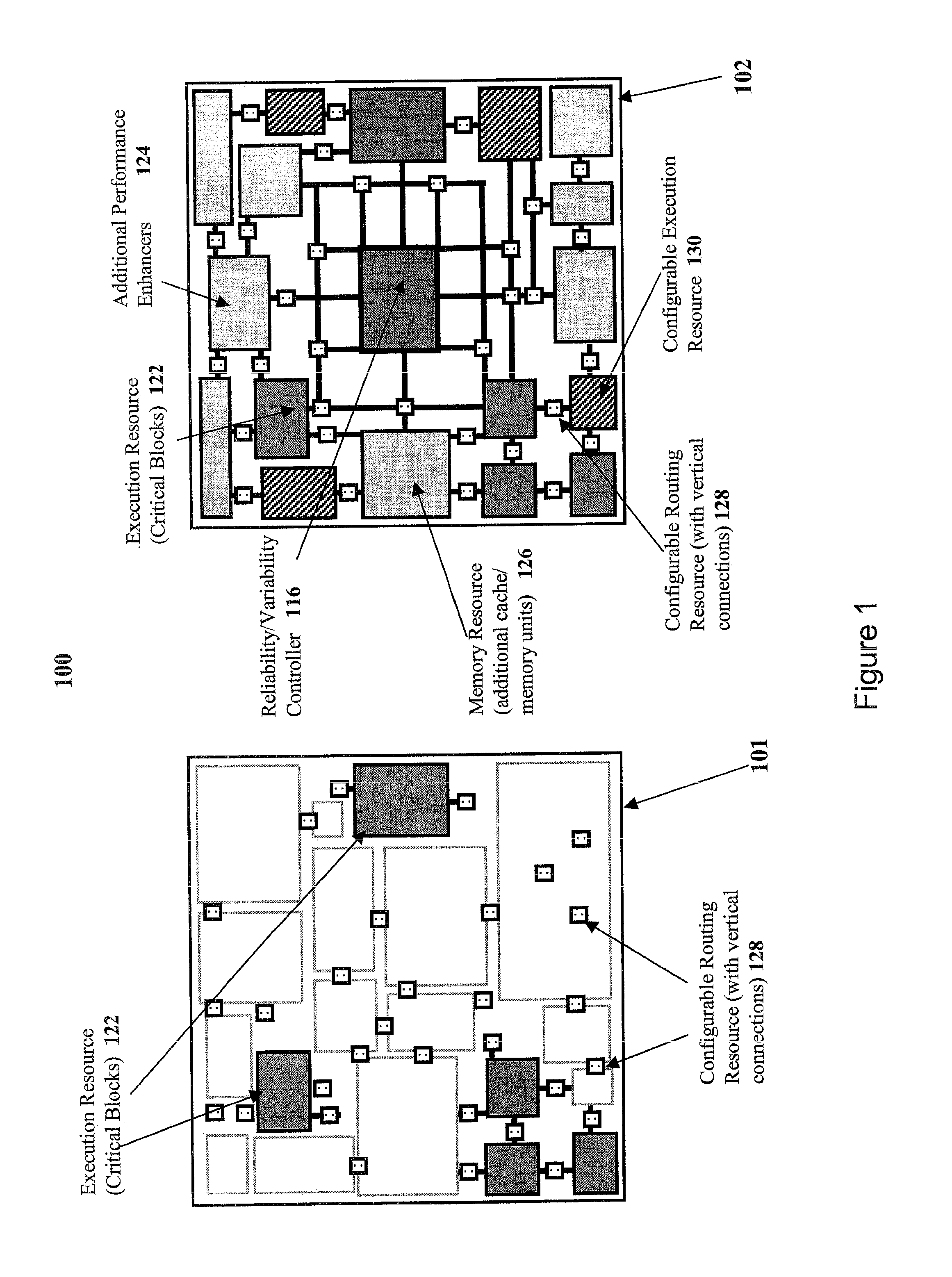
[0069]Referring now in detail to FIG. 2 of the drawings, the concept is represented on a 2-layer 3D embodiment 200, having first and second layers 101, 102. The second device layer 102 includes an on-chip variability / reliability controller 116, as well as redundant resources 218 that can be activated if a primary unit 220 in the first device layer 101 is faulty. The on-chip controller 116 activates any idle blocks while inactivating (turning off and by-passing) faulty units. Moreover, it includes performance-enhancing resources 122, 124, 126, 128, 130, additional cache / memory hierarchy such as DRAM or SRAM as well as monitoring and recovering capabilities.

[0070]The connection between the primary copy of a block and the redundancy which is placed on the top layer 102 may be achieved through vertical interconnects 128, such as TSVs (through-the-silicon-vias). The configurable interconnect 128 can be adjusted to connect either copy of the fault domains to the rest of the chip in case o...

embodiment 300

[0072]Referring now in detail to FIG. 3 of the drawings, the inventive concept is further represented on a 3-layer 3D embodiment 300, having first 101, second 102 and third 101 layers. In this embodiment, one auxiliary (or secondary) chip 102 is stacked in between two primary chips 101. The second device layer 102 includes an on-chip variability / reliability controller 116, as well as a configurable and custom redundant resource 330 that can be activated and dynamically assigned to either of the primary chips 101 if a primary unit 320 in either of the primary device layers 101 becomes faulty during system runtime. Also, if the primary units 320 in both primary chips 101 become faulty, the configurable redundant resource 330 on the secondary chip 102 can be used to replace both, albeit at a reduced system performance.

[0073]The additional device layer 102 includes the reliability / variability controller 116, with high-bandwidth and low-latency access to the rest of the chip. The reliabi...

first embodiment

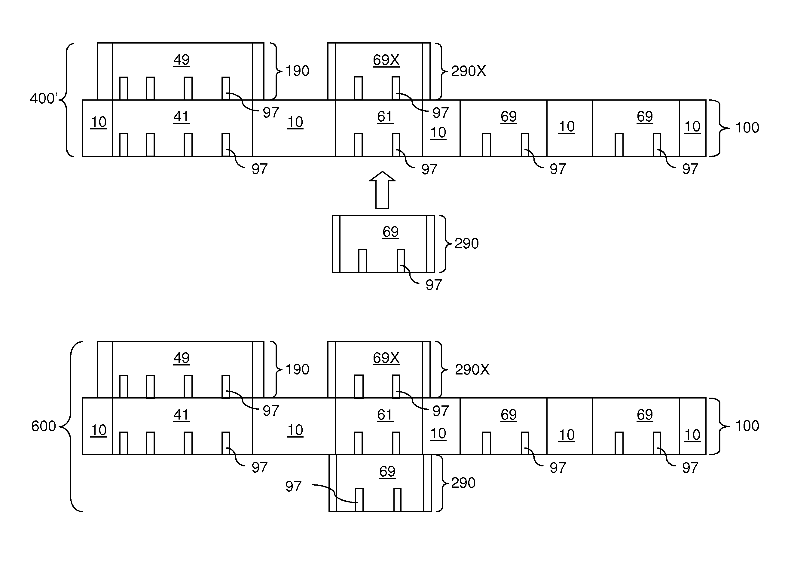
[0117]Referring to FIG. 8A, a base semiconductor chip 100 according to the present invention includes a non-functional first-type chiplet 41, a non-functional second-type chiplet 61, two functional second-type chiplets 69. The base semiconductor chip 100 may also include inter-chiplet regions 10 that separate the chiplets (41, 61, 69). A set of through-substrate vias 97 may be provided in each of the chiplets (41, 61, 91) in the base semiconductor chip 100. To compensate for the deficiency in the functionality of the base semiconductor chip 100 due to the non-functional chiplets, i.e., the non-functional first-type chiplet 41 and the non-functional second-type chiplet 61, a functional first-type repair semiconductor chip 190 and a functional second-type repair semiconductor chip 290 are stacked directly on the non-functional first-type chiplet 41 and the non-functional second-type chiplet 61, respectively. The functional first-type repair semiconductor chip 190 includes a functional...


PUM


Abstract

In one aspect, a method of enhancing semiconductor chip process variability and lifetime reliability through a three-dimensional (3D) integration applied to electronic packaging is disclosed. Also provided is an arrangement for implementing the inventive method. In another aspect, a method and on-chip controller are disclosed for enhancing semiconductor chip process variability and lifetime reliability through a three-dimensional (3D) integration applied to electronic packaging. Also provided is an on-chip reliability / variability controller arrangement for implementing the inventive method. In yet another aspect, base semiconductor chips, each comprising a plurality of chiplets, are manufactured and tested. For a base semiconductor chip having at least one non-functional chiplet, at least one repair semiconductor chiplet chiplet is vertically stacked. A functional multi-chip assembly is formed, which provides the same functionality as a base semiconductor chip in which all chiplets are functional.

Description

[0001]The present application is a continuation-in-part of, is related to, and claims the benefit of priority from, invented-by-the-same-inventors and commonly assigned U.S. application Ser. No. 11 / 947,207, filed on Nov. 29, 2007 and now abandoned, and Ser. No. 11 / 948,376, filed on Nov. 30, 2007 and now abandoned. The contents of U.S. application Ser. Nos. 11 / 947,207 and 11 / 948,376 are expressly incorporated herein. The present application is also related to a commonly assigned and co-pending U.S. application Ser. No. 12 / 041,878 filed on Mar. 4, 2008, the contents of which are incorporated herein by reference.FIELD OF THE INVENTION[0002]The present invention relates to a method for enhancing semiconductor chip process variability and lifetime reliability through three-dimensional (3D) integration and an arrangement for implementing the inventive method, and a control method and on-chip controller for enhancing semiconductor chip process variability and lifetime reliability through t...

Claims


Application Information

Patent Timeline
Patent Type & Authority Patents(United States)
IPC IPC(8): H01L21/66H01L21/00
CPCG01R31/31724H01L25/50H01L21/485G01R31/3172H01L22/14H01L2225/06596H01L22/20G06F11/20H01L2924/0002H01L21/76898H01L22/22H01L25/0657H01L2924/00
Inventor BOSE, PRADIPKURSUN, ERENRIVERS, JUDE A.ZYUBAN, VICTOR
Owner GLOBALFOUNDRIES INC
Why Eureka
Try Eureka