

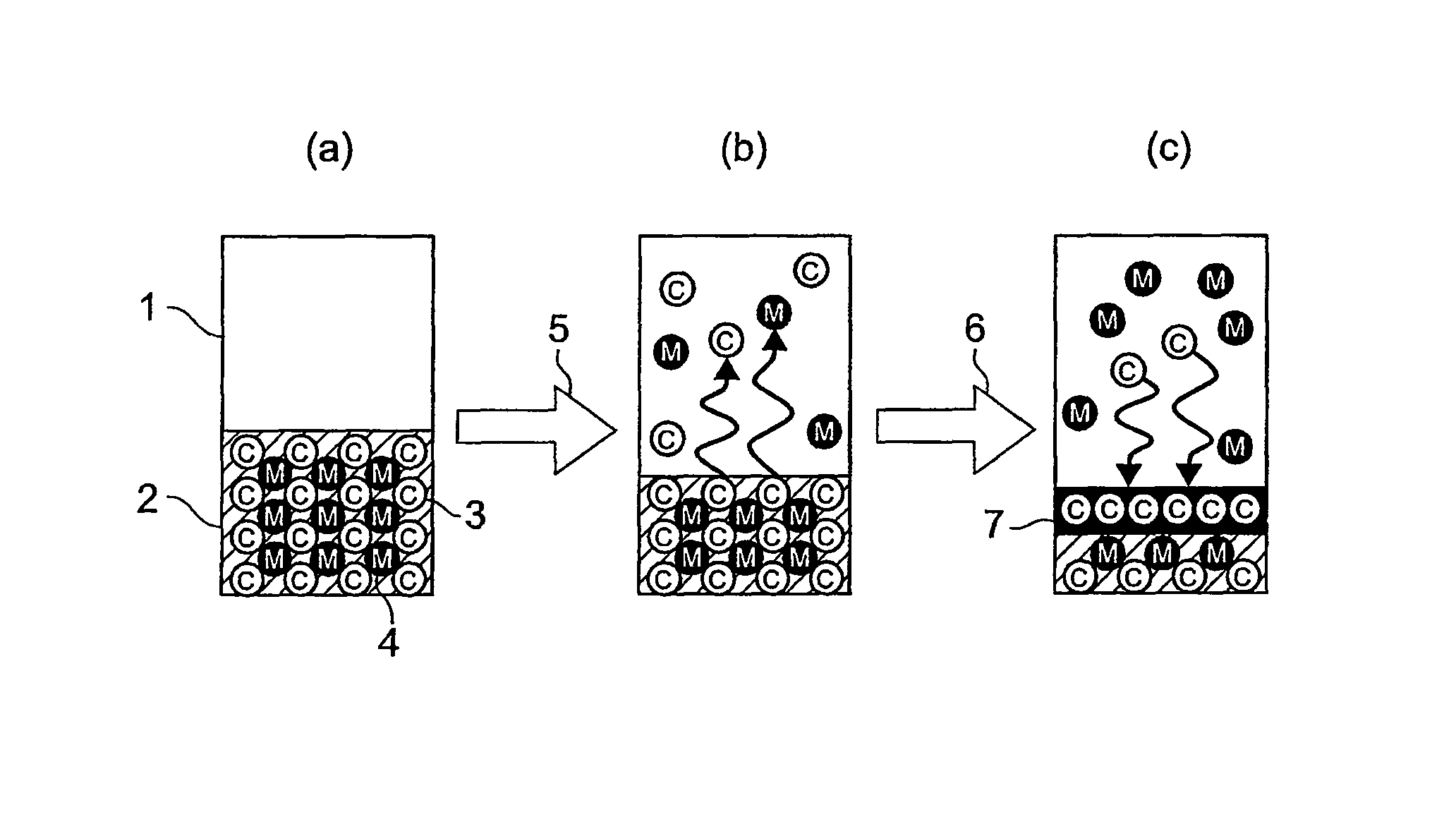
Manufacturing method of graphene substrate and graphene substrate
a technology of graphene substrate and manufacturing method, which is applied in the direction of graphene, material nanotechnology, graphene, etc., can solve the problems of over-the-counter manufacturing methods of graphene substrate, difficulty in mass production, and possible quality degradation, and achieves low manufacturing cost, high quality, and high productivity.
- Summary
- Abstract
- Description
- Claims
- Application Information
AI Technical Summary
Benefits of technology
Problems solved by technology
Method used
Image

Examples
example 1
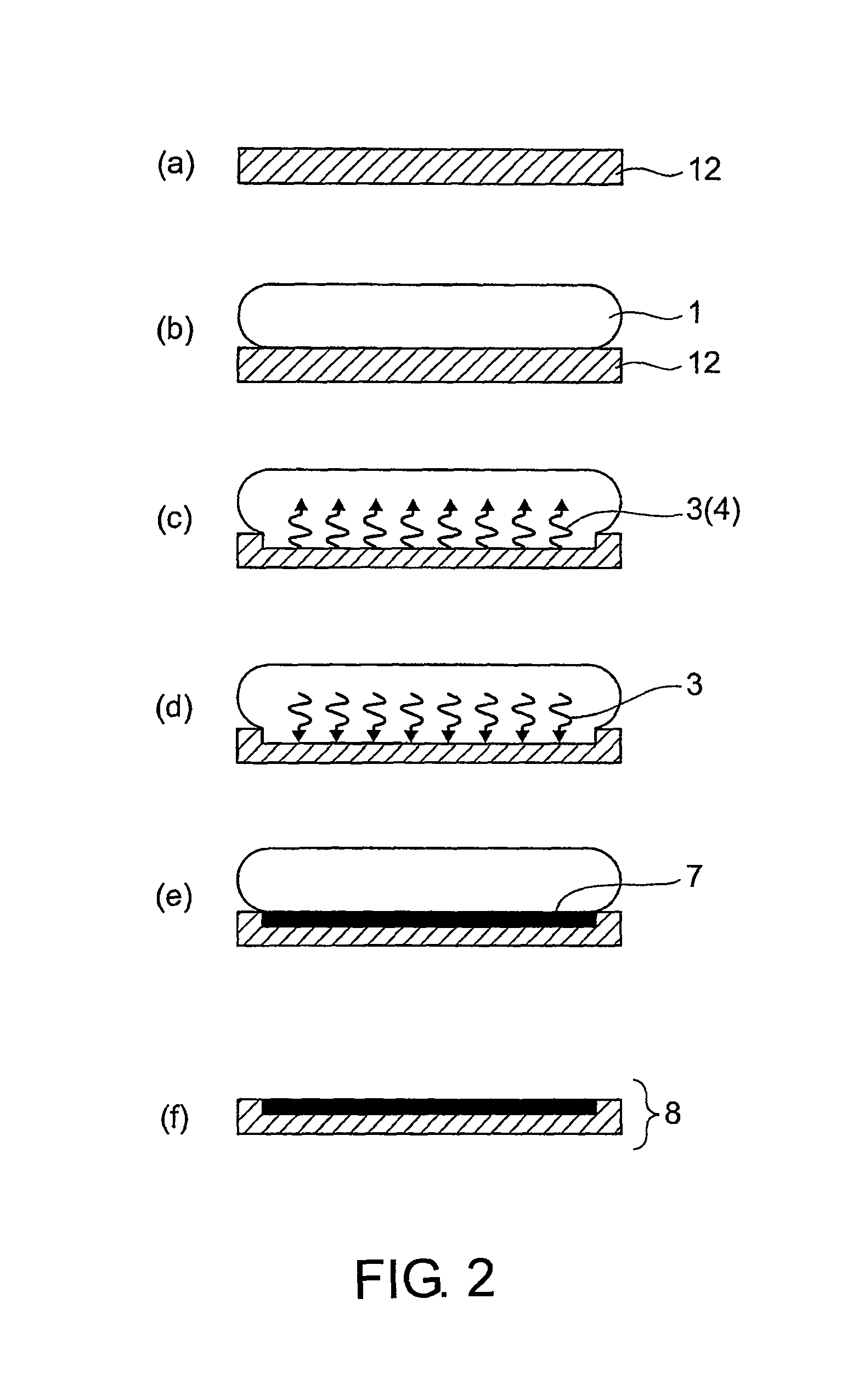
[0216]Graphene substrates 8a and 8b were fabricated at various heating temperatures by the method shown in FIG. 5, and relationship between heating temperature and structure of the graphene 7 in the graphene substrates 8a and 8b was investigated. Specific procedures are as described below.
[0217]Firstly, a silicon carbide substrate (6H—SiC / silicon surface, 10×10×0.45 mmt) was prepared as a substrate 12 (carbide layer 2) and a sapphire substrate (10×10×1 mmt) was prepared as a second substrate 20, and the substrates were washed with isopropyl alcohol and then with acetone.
[0218]The sapphire substrate was heated at 1000° C. in the atmosphere for one hour, whereby any carbon compounds were completely removed.
[0219]Subsequently, as shown in FIG. 5, the sapphire substrate was fit in the holder 21a, then 200 μl (microliters, corresponding to about 1 g) of molten gallium was placed on the sapphire substrate, and then a silicon carbide substrate was placed on the gallium.
[0220]Six such sampl...
example 2
[0232]The same procedures as Example 1 were used to manufacture graphene substrates 8a and 8b, except that the cooling time was varied while the heating temperature was fixed, and relationship between cooling speed and structure of the graphene 7 in the graphene substrates 8a and 8b thus obtained was investigate.
[0233]Specifically, six samples were prepared, and as shown in FIG. 9, graphene substrates 8a and 8b were manufactured with the heating temperature fixed to 1000° C. as an optimum temperature for growth of graphene, while the cooling time was set variously to (1) 0 minute, (2) 30 minutes, (3) 60 minutes, (4) 90 minutes, (5) 120 minutes, (6) 150 minutes, and (7) 180 minutes. The other conditions were the same as the conditions in Example 1.
[0234]The term “cooling time” as used herein means a period of time required to cool from 1000° C. to 800° C.
[0235]Then, the state of graphene formation on the surface of each of the silicon carbide substrate (graphene substrate 8a) and the...
example 3
[0238]Graphene substrates were fabricated on various carbide substrates (substrates 12) having different compositions under various heating temperature conditions, and relationship between heating temperature conditions and types of carbide making up the carbide substrates was evaluated. Specifically, the evaluation was conducted according to procedures as described below.
[0239]A plurality of substrates 12 (with a carbide layer 2) were prepared, consisting of a substrate with a 6H—SiC / carbon surface, one with a 4H—SiC / silicon surface, and one with a 4H—SiC / carbon surface, a tungsten carbide substrate, and a titanium carbide substrate, and graphene substrates 8 were fabricated from these substrates 12 under the same various heat treatment conditions as those of Example 1.
[0240]The results are shown in FIG. 10.
[0241]FIG. 10 is a graph showing, on temperature profiles, ranges of heating temperature and cooling time suitable for manufacture of graphene substrates according to the invent...
PUM
| Property | Measurement | Unit |
|---|---|---|
| temperature | aaaaa | aaaaa |
| thickness | aaaaa | aaaaa |
| thickness | aaaaa | aaaaa |
Abstract
Description
Claims
Application Information