Layout correcting method and layout correcting system

a layout and correcting method technology, applied in the field of layout correcting methods and layout correcting systems, can solve the problems of affecting the product yield, the estimated hotspots are far from the real electrical performance of the product, and possible errors in any of the multiple stages, so as to achieve accurate correction of the integrated circuit design layout

Active Publication Date: 2015-01-06
UNITED MICROELECTRONICS CORP
View PDF9 Cites 0 Cited by
  • Summary
  • Abstract
  • Description
  • Claims
  • Application Information

AI Technical Summary

Benefits of technology

[0007]The disclosure is directed to a layout correcting method and a layout correcting system, a direct probing process is performed on the devices under test for considering the surrounding environments and a smarting sizing is performed for accurately correcting the integrated circuit design layout.

Problems solved by technology

Generally, some defects are possibly generated in any of the multiple stages.
If the defect is found after the integrated circuit product is fabricated, it is necessary to identify the source of problems from the beginning.
However, since the conventional method lacks systematical and hierarchical analyses, the estimated hotspots are far from the real electrical performance of the product.
Under this circumstance, the product yield is usually unsatisfied.
Moreover, analyzing layout dependent effect (LDE) on circuit performance is a big challenge.
It is hard to consider process and circuit layout interaction once the machine / processing conditions are changed.

Method used


Image

  • Layout correcting method and layout correcting system
  • Layout correcting method and layout correcting system
  • Layout correcting method and layout correcting system

Examples


Embodiment Construction

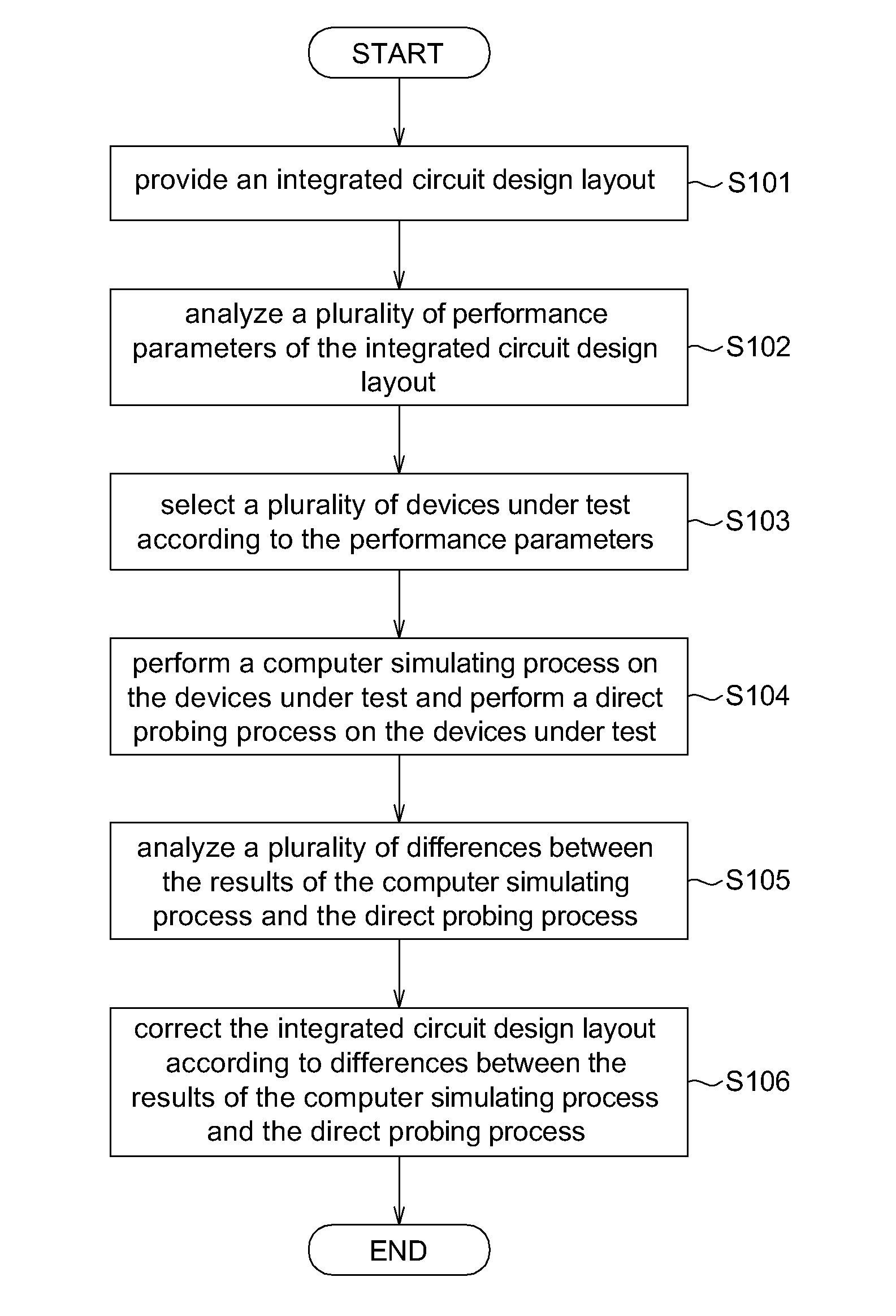
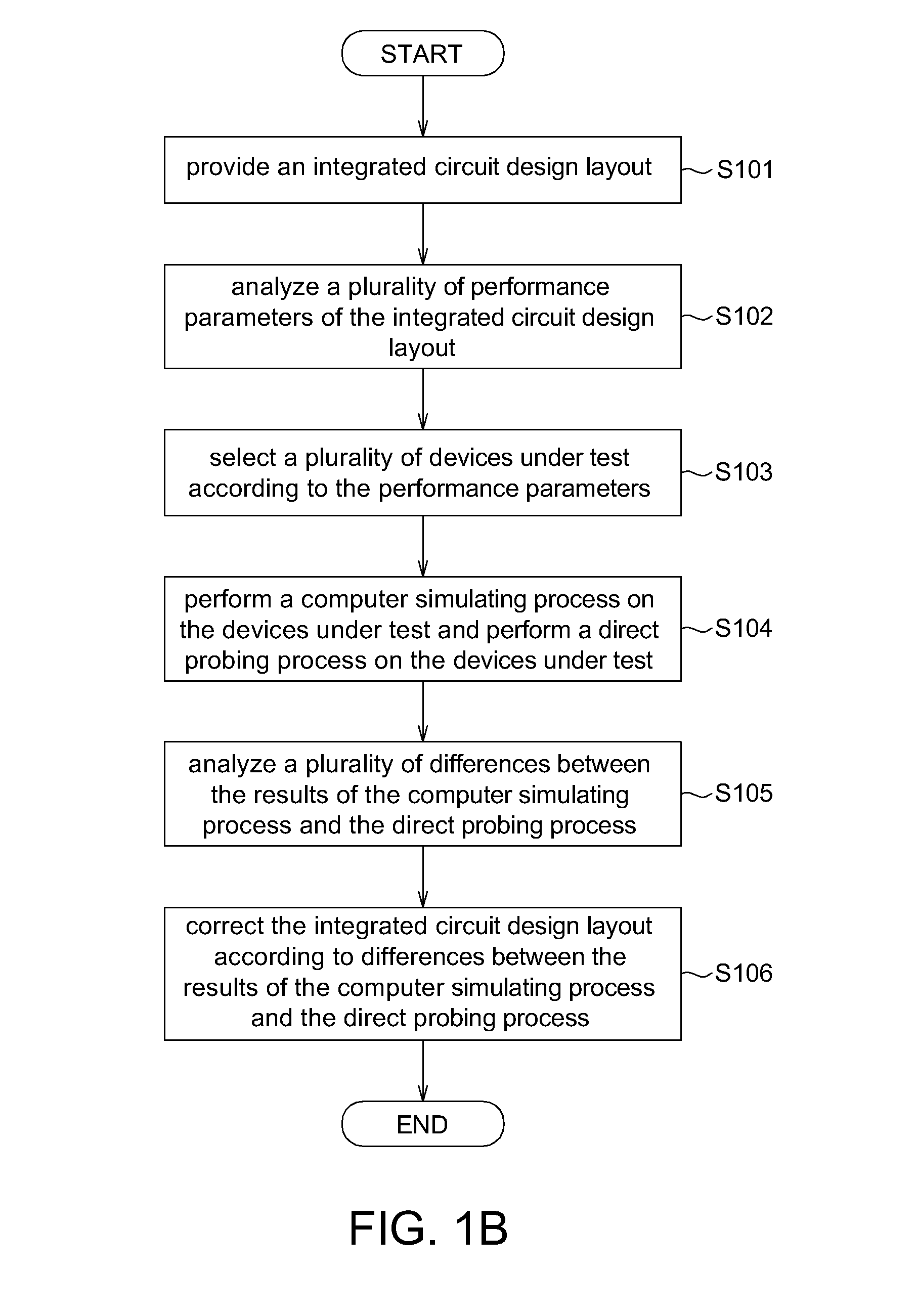
[0017]Preferred embodiments are disclosed below for elaborating the invention. A direct probing process is performed on the devices under test for considering the surrounding environments and a smarting sizing is performed for accurately correcting the integrated circuit design layout. The following embodiments are for the purpose of elaboration only, not for limiting the scope of protection of the invention. Besides, secondary elements are omitted in the following embodiments to highlight the technical features of the invention.

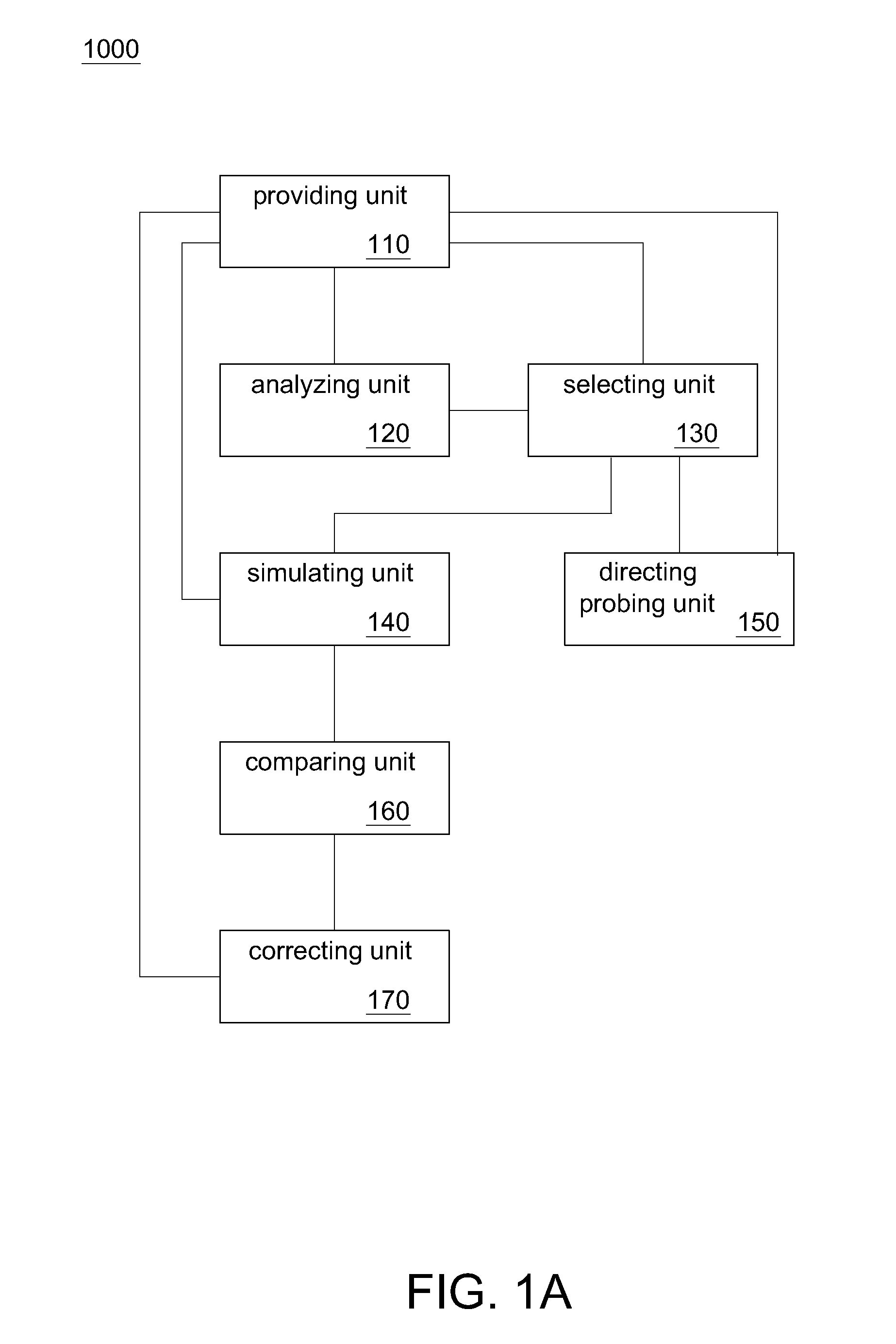
[0018]Please referring to FIG. 1A, a block diagram of a layout correcting system 100 is shown. The layout correcting system 1000 can be a combination of a plurality of electronic equipments, a personal computer, a circuit board, a chip or a circuit having a function for correcting layout. The layout correcting system 1000 includes a providing unit 110, an analyzing unit 120, a selecting unit 130, a simulating unit 140, a directing probing unit 150, a compari...


PUM


Abstract

A layout correcting method and a layout correcting system are provided. The layout correcting method includes the following steps. An integrated circuit design layout is provided. A plurality of performance parameters of the integrated circuit design layout are analyzed. A plurality of devices under test is selected according to the performance parameters. A computer simulating process is performed on the devices under test and a direct probing process is performed on the devices under test. The direct probing process is an on-chip test for comparing each device under test and an environment condition thereof by a Boolean algebra algorithm. A plurality of differences between the results of the computer simulating process and the direct probing process is analyzed. The integrated circuit design layout is corrected according to differences between the results of the computer simulating process and the direct probing process.

Description

BACKGROUND[0001]1. Technical Field[0002]The disclosure relates in general to a correcting method and a correcting system, and more particularly to a layout correcting method and a layout correcting system.[0003]2. Description of the Related Art[0004]As known, it takes multiple stages to fabricate an integrated circuit product from the beginning of designing the integrated circuit. Generally, some defects are possibly generated in any of the multiple stages. If the defect is found after the integrated circuit product is fabricated, it is necessary to identify the source of problems from the beginning. Under this circumstance, the speed of launching the product will be slowed down.[0005]For solving these drawbacks, a simple rule (e.g. a minimum critical dimension) or a physical model is conventionally used in the circuit design layout in order to sieve out the area that is unable to tolerate the process variation. In such way, the hotspots prone to error in mass production can be iden...

Claims


Application Information

Patent Timeline
Patent Type & Authority Patents(United States)
IPC IPC(8): G06F17/50
CPCG06F17/5081G06F30/398
Inventor HOU, HSIN-MINGKUNG, JI-FU
Owner UNITED MICROELECTRONICS CORP
Why Eureka
Try Eureka