Optical device structure using GaN substrates for laser applications

a technology of optical devices and substrates, applied in the direction of lasers, semiconductor laser structural details, semiconductor lasers, etc., can solve the problems of high cost, large size, weight, and cost of conventional light bulbs, and achieve the effects of improving device performance, simple and cost effective, and reducing the cost of lasers

Active Publication Date: 2015-06-30
KYOCERA SLD LASER INC
View PDF282 Cites 13 Cited by
  • Summary
  • Abstract
  • Description
  • Claims
  • Application Information

AI Technical Summary

Benefits of technology

[0019]In a specific embodiment, the invention provides a laser device comprising a gallium and nitrogen containing substrate having a surface region configured in a non-polar orientation, an active region comprising at least five quantum well regions and at least four thin barrier regions configured to separate respective first quantum well region, second quantum well region, third quantum well region, fourth quantum well region, and fifth quantum well region. That is, a first barrier region separates the first from the second quantum well region, a second barrier region separates the second quantum well region from the third quantum well region, a third barrier region separates the third quantum well region from the fourth quantum well region, and the fourth barrier region separates the fourth quantum well region from the fifth quantum well region. In a preferred embodiment, each of the barrier regions is thin and is characterized by a thickness of 2.5 nm and less, which leads to reduced overall strain in the active region including both the quantum well regions and barrier regions. As used herein, the second, third, and fourth quantum well regions are configured within the first and fifth quantum well regions, which are configured within a vicinity of exterior portions of the active region. Of course, one of ordinary skill in the art would recognize that there may be more than five quantum well regions or fewer than five quantum well regions.
[0021]The present invention enables a cost-effective optical device for laser applications. In a specific embodiment, the present optical device can be manufactured in a relatively simple and cost effective manner. Depending upon the embodiment, the present apparatus and method can be manufactured using conventional materials and / or methods according to one of ordinary skill in the art. The present laser device uses a nonpolar gallium nitride material capable of achieving a laser having a wavelength of about 400 nanometers to about 500 nanometers and greater, among others. In other embodiments, the device and method can achieve a wavelength of about 500 nanometers and greater including 520 nanometers to about 540 nanometers. In a specific embodiment, the method and device can achieve a wavelength of 435 to 470 nanometers, among others. In a preferred embodiment, the single lateral mode laser device is characterized by a wall plug efficiency (optical power out / electrical power in) of about 14-25% in the 50 to 150 mW output power range for a laser configured on a non-polar gallium and nitrogen containing material. The wall plug efficiency of the single lateral mode laser device can be characterized by values greater than 20%. In such embodiments, the electrical power may range from about 50 mW to about 200 mW and can be greater such as 200 mW to about 500 mW and can be others. In other embodiments, the present laser device configured on a semi-polar substrate orientation (e.g., {20-21}, slightly offcut {20-21}) provides wall plug efficiencies of 6% to 12% and greater for emission of 520 nanometers and greater. In a specific embodiment, the present device can be configured as a single lateral mode or multi-mode devices. In a preferred embodiment, the present single lateral mode device has a wall plug efficiency of 15 to 25% and may be at least 1.5 to 2× higher than conventional single lateral mode devices operating in the 435 to 470 nanometer range. In a preferred embodiment, the present laser devices uses a multi-quantum well structure configured with thin barrier regions for improved device performance, including higher wall plug efficiency and desirable other desirable electrical properties. Depending upon the embodiment, one or more of these benefits may be achieved. These and other benefits may be described throughout the present specification and more particularly below.

Problems solved by technology

Unfortunately, drawbacks exist with the conventional Edison light bulb:The conventional light bulb dissipates much thermal energy.
More than 90% of the energy used for the conventional light bulb dissipates as thermal energy.Reliability is an issue since the conventional light bulb routinely fails often due to thermal expansion and contraction of the filament element.Light bulbs emit light over a broad spectrum, much of which does not result in bright illumination or due to the spectral sensitivity of the human eye.Light bulbs emit in all directions and are not ideal for applications requiring strong directionality or focus such as projection displays, optical data storage, or specialized directed lighting.
The Ar-ion laser had the benefit of producing highly directional and focusable light with a narrow spectral output, but the efficiency, size, weight, and cost of the lasers were undesirable.
As laser technology evolved, more efficient lamp pumped solid state laser designs were developed for the red and infrared wavelengths, but these technologies remained a challenge for blue and green and blue lasers.
The resulting green and blue lasers were called “lamped pumped solid state lasers with second harmonic generation” (LPSS with SHG) and were more efficient than Ar-ion gas lasers, but were still too inefficient, large, expensive, fragile for broad deployment outside of specialty scientific and medical applications.
Additionally, the gain crystal used in the solid state lasers typically had energy storage properties which made the lasers difficult to modulate at high speeds which limited its broader deployment.
However, the change to diode pumping increased the system cost and required précised temperature controls, leaving the laser with substantial size, power consumption while not addressing the energy storage properties which made the lasers difficult to modulate at high speeds.
These lasers designs are meant to improve the efficiency, cost and size compared to DPSS-SHG lasers, but the specialty diodes and crystals required make this challenging.
Additionally, while the diode-SHG lasers have the benefit of being directly modulate-able, they suffer from severe sensitivity to temperature which limits their application.

Method used


Image

  • Optical device structure using GaN substrates for laser applications
  • Optical device structure using GaN substrates for laser applications
  • Optical device structure using GaN substrates for laser applications

Examples


examples

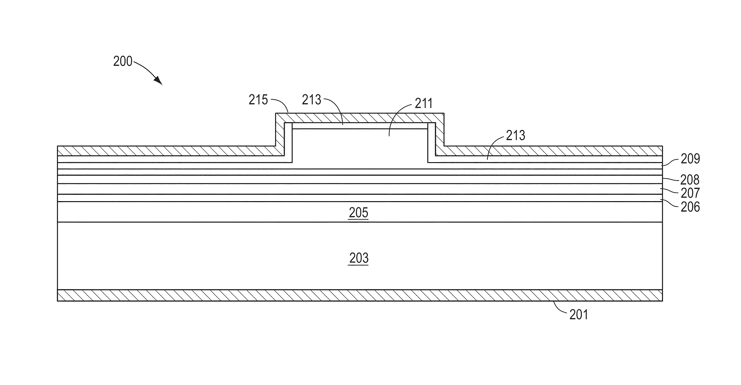
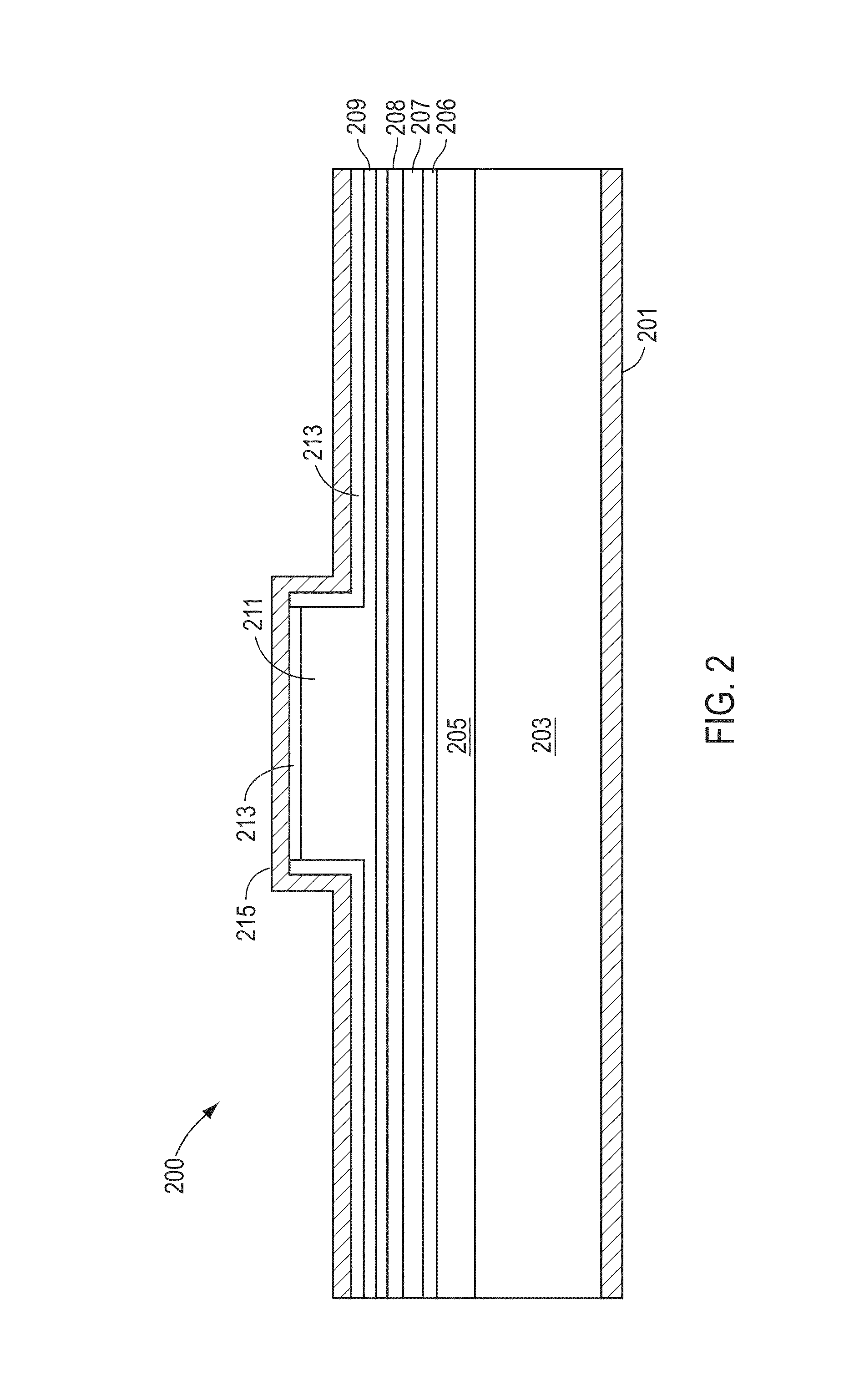
[0094]FIG. 13 is a simplified diagram illustrating a laser device according to one or more examples of the present invention. This diagram is merely an illustration and should not unduly limit the scope of the claims herein. One of ordinary skill in the art would recognize other variations, modifications, and alternatives. In this example, the optical device includes a gallium nitride substrate member having a nonpolar crystalline surface region characterized by an orientation of about + / −1 degree towards (0001) and less than about 0.3 degrees towards (11-20). The bulk GaN substrate has a surface dislocation density below 1E5 to 1E7 cm-2 or about 1E6 cm−2 and a surface roughness of less than 0.2 nm.

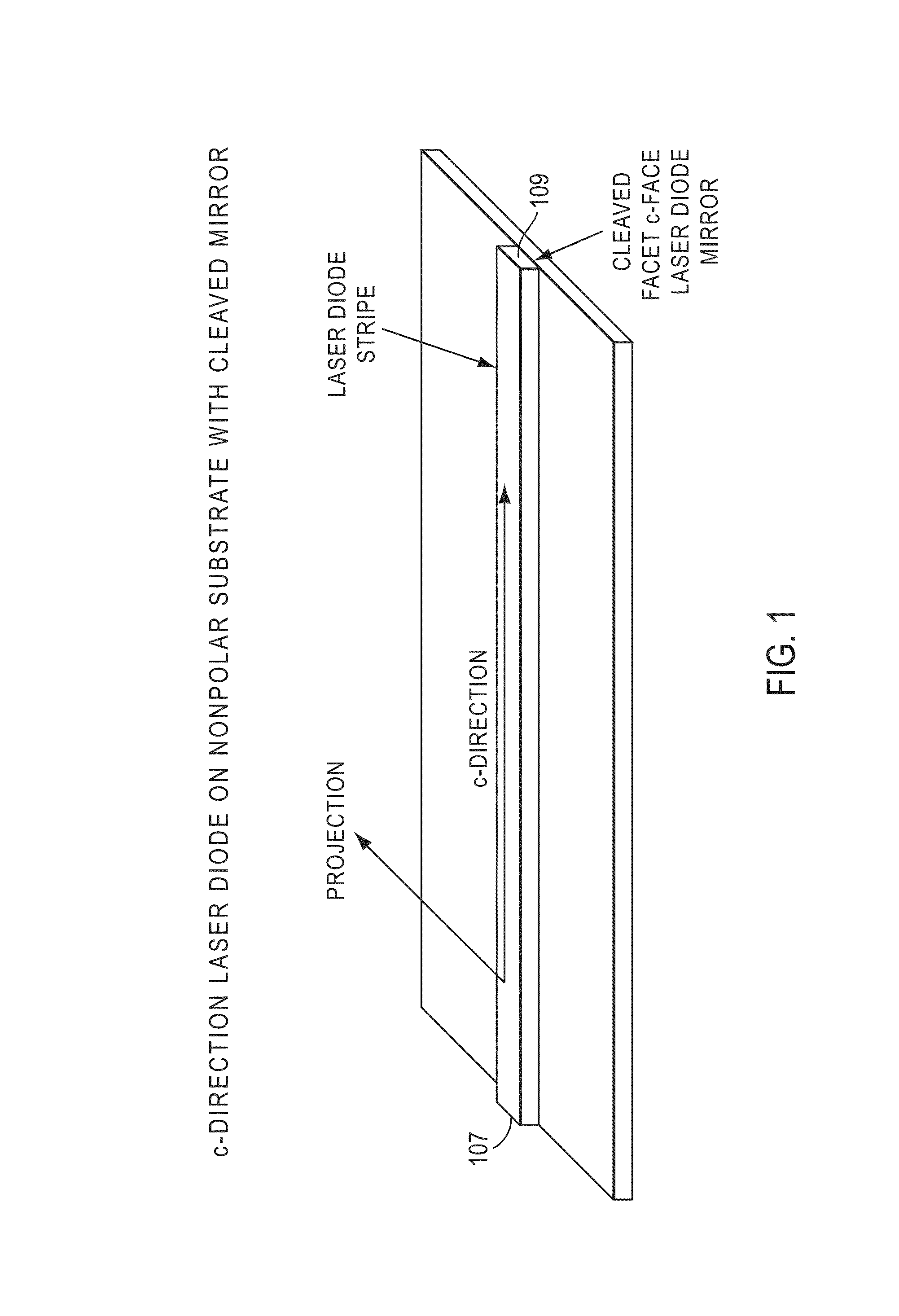
[0095]The device has a laser stripe region formed overlying a portion of the nonpolar crystalline orientation surface region. The laser stripe region is characterized by a cavity orientation is substantially parallel to the c-direction and has a first end and a second end. The device has ...


PUM


Abstract

An optical device includes a gallium nitride substrate member having an m-plane nonpolar crystalline surface region characterized by an orientation of about −1 degree towards (000-1) and less than about + / −0.3 degrees towards (11-20). The device also has a laser stripe region formed overlying a portion of the m-plane nonpolar crystalline orientation surface region. In a preferred embodiment, the laser stripe region is characterized by a cavity orientation that is substantially parallel to the c-direction, the laser stripe region having a first end and a second end. The device includes a first cleaved c-face facet, which is coated, provided on the first end of the laser stripe region. The device also has a second cleaved c-face facet, which is exposed, provided on the second end of the laser stripe region.

Description

CROSS-REFERENCE TO RELATED APPLICATIONS[0001]This application is a continuation of U.S. Ser. No. 12 / 868,441, filed Aug. 25, 2010, which is a continuation-in-part of U.S. Ser. No. 12 / 759,273, filed Apr. 13, 2010; which claims priority to U.S. Ser. No. 61 / 168,926, filed Apr. 13, 2009; and U.S. Ser. No. 61 / 243,502, filed Sep. 17, 2009, each of which is commonly assigned and hereby incorporated by reference herein.BACKGROUND OF THE INVENTION[0002]This invention is directed to optical devices and related methods. More particularly, the invention provides a method and device for emitting electromagnetic radiation using nonpolar gallium containing substrates such as GaN, AlN, InN, InGaN, AlGaN, and AlInGaN, and others. The invention can be applied to optical devices, lasers, light emitting diodes, solar cells, photoelectrochemical water splitting and hydrogen generation, photodetectors, integrated circuits, and transistors, as well as other devices.[0003]In the late 1800's, Thomas Edison i...

Claims


Application Information

Patent Timeline
Patent Type & Authority Patents(United States)
IPC IPC(8): H01S5/00H01S5/02H01S5/343B82Y20/00H01S5/22H01S5/028H01S5/32H01L21/02H01S5/20
CPCH01S5/2201H01S5/0202H01S5/34333B82Y20/00H01L21/02389H01L21/02433H01L21/0254H01S5/028H01S5/0287H01S5/2009H01S5/3202H01S5/32025
Inventor RARING, JAMES W.FEEZELL, DANIEL F.PFISTER, NICHOLAS J.SHARMA, RAJATSCHMIDT, MATHEW C.ELSASS, CHRISTIANE POBLENZCHANG, YU-CHIA
Owner KYOCERA SLD LASER INC
Why Eureka
Try Eureka