Chemical mapping using thermal microscopy at the micro and nano scales

a thermal microscopy and micro-nanometer technology, applied in the field of micro- and nano-scale photothermal chemical imaging, can solve the problems of not being very useful for organic compound identification, limited practical resolution limit to about 20 m, and not always well suited to the length scale involved in microfabricated devices, etc., to reduce the size of the heated spot, and reduce the cost of operation

Active Publication Date: 2015-07-28
THE UNITED STATES OF AMERICA AS REPRESENTED BY THE SECRETARY OF THE NAVY
View PDF12 Cites 27 Cited by
  • Summary
  • Abstract
  • Description
  • Claims
  • Application Information

AI Technical Summary

Benefits of technology

[0012]In another approach, focused electron or ion beams are used instead of infrared lasers to further decrease the size of the heated spot. This way, spatial resolutions well below 1 micron (to as low as 1 nm) are possible.
[0013]The purpose of the present invention is to provide a new non-contact and non-destructive imaging technique that eliminates the need for sample preparation and provides similar content information as FTIR or Raman spectroscopy (i.e. molecular information) while mitigating any fluorescence and luminescence effects, and offers rapid scan rates and / or higher spatial resolution. In one approach, it utilizes photo-thermal heating of the sample with a quantum cascade laser (or other suitable infrared laser) and measures the resulting increase in thermal emissions by either an infrared (IR) detector or a laser probe having a visible laser reflected from the sample. The latter case allows for further increases in the spatial resolution from ˜10 μm to ˜1 μm or better, with suitable experimental conditions. Since the thermal emission signal is proportional to the absorption coefficient at a given laser wavelength, by tuning the wavelength of the IR laser the IR absorption spectrum of the sample can be inferred from the thermal emission. By raster scanning over the surface of the sample, maps of the chemical composition of the sample surface can be obtained.

Problems solved by technology

Existing established techniques are not always well suited for the length scales involved in microfabricated devices.
While FTIR micro-spectroscopy addresses this problem, the practical resolution limit is limited to about 20 μm.
X-ray mapping can achieve higher resolution but provides elemental maps, though this is not very useful for identification of organic compounds.
On the other hand, well-developed imaging techniques with nanometer resolution capability (e.g. SPM, AFM, TEM / EELS) are often impractical to operate at the micron-scale.
These techniques, operated at the nanometer scale, typically offer a limited physical footprint scan range, operate well with samples exhibiting only a limited range of surface roughness, and routinely require sample preparation.
However, the process is inefficient and the signal response levels are extremely low, necessitating long integration times at each point, leading to long scan times and necessitating the use of expensive high performance detectors.
In addition, samples which fluoresce cannot be practically characterized with Raman imaging.
However, the spatial resolution of this technique is diffraction limited by the long wavelength of the heating source and the thermal emission.

Method used


Image

  • Chemical mapping using thermal microscopy at the micro and nano scales
  • Chemical mapping using thermal microscopy at the micro and nano scales
  • Chemical mapping using thermal microscopy at the micro and nano scales

Examples


Embodiment Construction

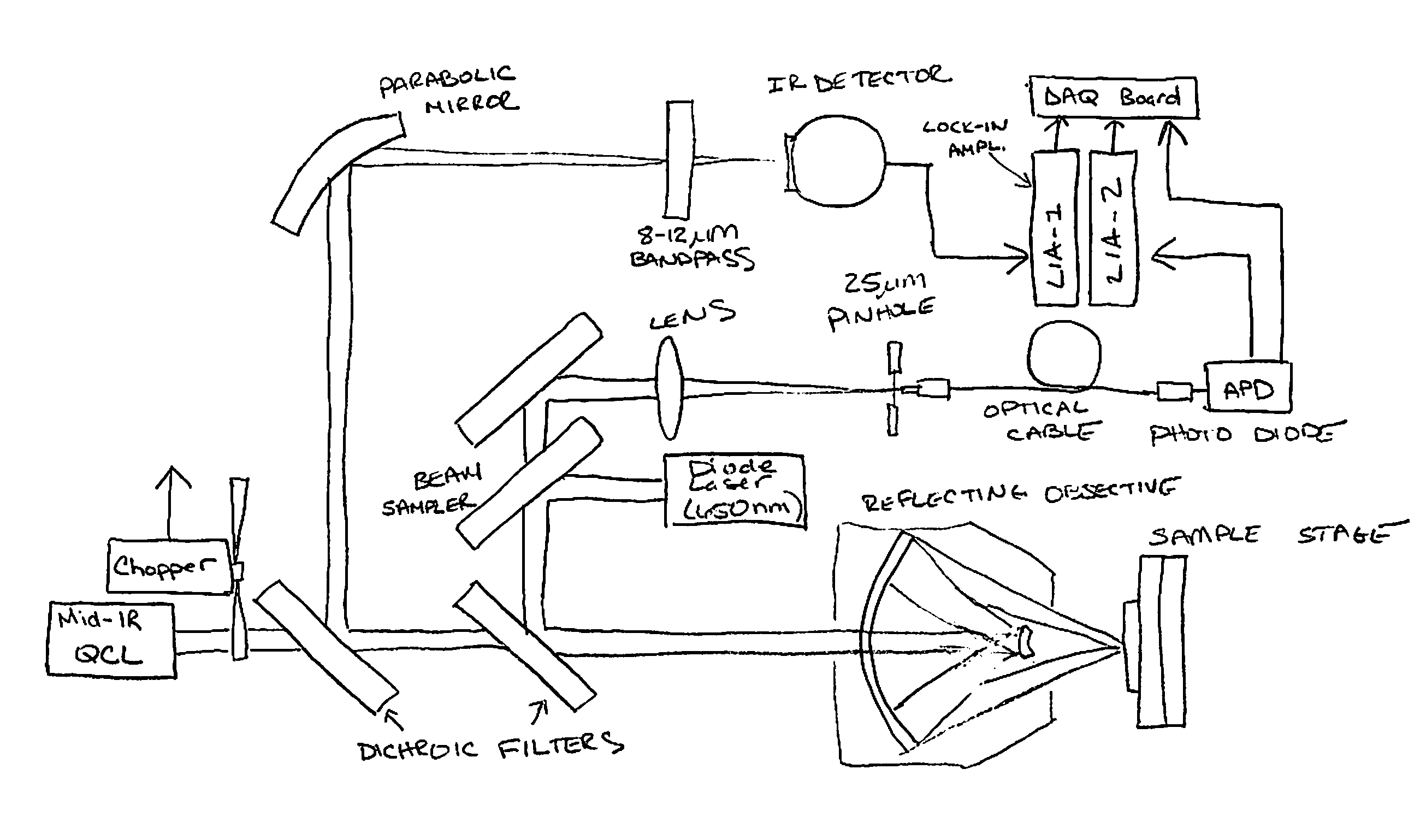
[0030]One embodiment of the present invention uses a three-in-one instrument comprising a diffraction-limited PT microscope with an IR light detector, a sub-diffraction-limited PT microscope with visible light detector, and a standard confocal microscope (see FIG. 1). A sample undergoes photo-thermal heating using an IR laser and the resulting increase in thermal emissions is measured with either the IR detector or a laser probe having a visible laser reflected from the sample. The visible laser probe (operated in continuous wave (cw) mode) is co-focused with the IR beam at the sample. As the sample is periodically heated, the sample expands and contracts, with its surface moving up and down which modulates the reflected visible laser. The index of the refraction of the sample also changes and this is also registered as a change in reflectance. This modulation is demodulated by employing a lock-in detector.

Photo-Thermal Confocal Microscope

[0031]FIG. 1 shows the schematic drawing of ...


PUM

PropertyMeasurementUnit
wavelength rangeaaaaaaaaaa
wavelengthsaaaaaaaaaa

Abstract

A non-destructive method for chemical imaging with ˜1 nm to 10 μm spatial resolution (depending on the type of heat source) without sample preparation and in a non-contact manner. In one embodiment, a sample undergoes photo-thermal heating using an IR laser and the resulting increase in thermal emissions is measured with either an IR detector or a laser probe having a visible laser reflected from the sample. In another embodiment, the infrared laser is replaced with a focused electron or ion source while the thermal emission is collected in the same manner as with the infrared heating. The achievable spatial resolution of this embodiment is in the 1-50 nm range.

Description

PRIORITY CLAIM[0001]This Application claims priority from U.S. Provisional Application No. 61 / 563,665 filed on Nov. 25, 2011 by Robert Furstenberg et al., entitled “Method of Chemical Imaging Using a Novel Confocal Photo-Thermal Microscopy Technique,” the entire contents of which are incorporated herein by reference.BACKGROUND OF THE INVENTION[0002]1. Field of the Invention[0003]The present invention relates generally to chemical imaging and, more specifically, to microscopic and nanoscopic photo-thermal chemical imaging.[0004]2. Description of the Prior Art[0005]With the increasing materials complexity of microfabricated devices, there is a growing need for new characterization techniques that provide chemical composition with improved spatial resolution over relevant scales. Existing established techniques are not always well suited for the length scales involved in microfabricated devices. For example, FTIR spectroscopy provides averaged chemical composition information for milli...

Claims


Application Information

Patent Timeline
Patent Type & Authority Patents(United States)
IPC IPC(8): G01J5/02G01J3/02G01J5/60G02B21/00G01J3/28G01N21/17G01N21/3563G01N21/41G01N21/45G01N21/39
CPCG01J3/2823G01J3/02G01J5/60G01N21/171G02B21/008G02B21/0028G01N21/3563G01N21/41G01N21/45G01N2021/1714G01N2021/1725G01N2021/1731G01N2021/393G01J3/0202G01J3/443G01J3/45G01J2003/2826
Inventor FURSTENBERG, ROBERTKENDZIORA, CHRISBASSIM, NABIL D.MCGILL, ROBERT ANDREWNGUYEN, VIET K.
Owner THE UNITED STATES OF AMERICA AS REPRESENTED BY THE SECRETARY OF THE NAVY
Why Eureka
Try Eureka