Laser processing method and production method of multilayer flexible printed wiring board using laser processing method

a multi-layer flexible, laser processing technology, applied in metal-working apparatuses, resistive material coatings, metallic material coating processes, etc., can solve the problems of reducing affecting the reliability of the interlayer conduction path, and difficulty in forming a via of high reliability. achieve the effect of high reliability

Active Publication Date: 2015-09-29
NIPPON MEKTRON LTD
View PDF10 Cites 6 Cited by
  • Summary
  • Abstract
  • Description
  • Claims
  • Application Information

AI Technical Summary

Benefits of technology

[0045]With the present invention, a via hole is formed in as few shots as possible, without causing a resin residue in a via hole and causing the deformation and penetration of an internal layer circuit pattern exposed into the via hole.
[0046]According to an aspect of the present invention, there is provided a laser processing method of forming a via hole having a conductive film exposed in a bottom surface, by removing processed layers formed on the conductive film forming an internal circuit pattern by a laser, the processed layers including a first insulating layer and a second insulating layer, the first insulating layer provided with a conformal mask on a top surface thereof and having a first absorbance in an operational wavelength range of a processing laser and a first decomposition temperature, and the second insulating layer provided below the first insulating layer and having a second absorbance higher than the first absorbance in the operational wavelength range and a second decomposition temperature lower than the first decomposition temperature, the method including: radiating one shot of pulsed light having a first energy density that can remove the first insulating layer of the processed layers by one shot without causing a deformation and penetration of the conductive film; and subsequently radiating pulsed light having a second energy density that is lower than the first energy density and can remove a rest of the processed layers by a predetermined number of shots without causing a deformation and penetration of the conductive film.
[0048]With these features, the present invention provides the following effects.
[0049]Since the first insulating layer of a processed layer is completely removed by the first shot, a burr part does not occur in the first insulating layer. Therefore, it is possible to prevent an occurrence of a resin residue due to the burr part. Also, since the burr part does not occur, it is possible to reduce the total number of shots, which is required to form a via hole, as much as possible.
[0051]Further, as a result of suppressing a resin residue and the expansion of asperities of via hole side walls, plating adhesion to the internal wall of the via hole is improved and it is possible to form a via of high reliability.

Problems solved by technology

However, in the related art, when the processed layer is formed of multiple materials of different workability, for example, since a resin remains in the via hole, it is difficult to form a via of high reliability.
In such a case, subsequent laser processing is largely blocked.
As a result, plating adhesion to the internal walls of the step via hole and skip via hole degrades, which is a cause of degrading the reliability of an interlayer conduction path.
However, when the number of shots of pulsed laser is increased, there arises a problem that the productivity decreases.
3B(6), discontinuous parts occur in plate layers formed on the side walls, which is a cause of degrading the via reliability.
However, in a case where the copper foil 162 forming the internal layer circuit pattern 164 is thin (for example, equal to or below 12 the pulsed light penetrates the copper foil, which is a cause of an occurrence of short defect.
This space part causes a discontinuous part in the plate layer formed on the side wall of the step via hole, which is a cause of degrading the reliability of the step via.
However, to continuously radiate pulsed light to the identical part, the heat amount accumulated in the radiated part becomes large.
However, the polyamide adhesive is more expensive than the epoxy or acrylic adhesive which is generally used for a multilayer flexible printed wiring board.
Therefore, there is a problem that the production cost increases.

Method used


Image

  • Laser processing method and production method of multilayer flexible printed wiring board using laser processing method
  • Laser processing method and production method of multilayer flexible printed wiring board using laser processing method
  • Laser processing method and production method of multilayer flexible printed wiring board using laser processing method

Examples


embodiment 1

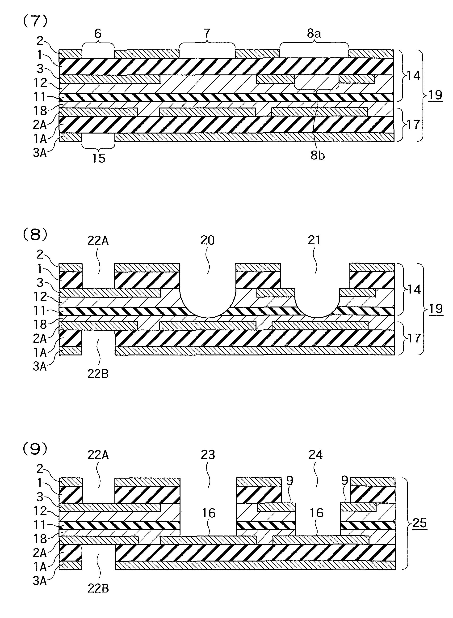
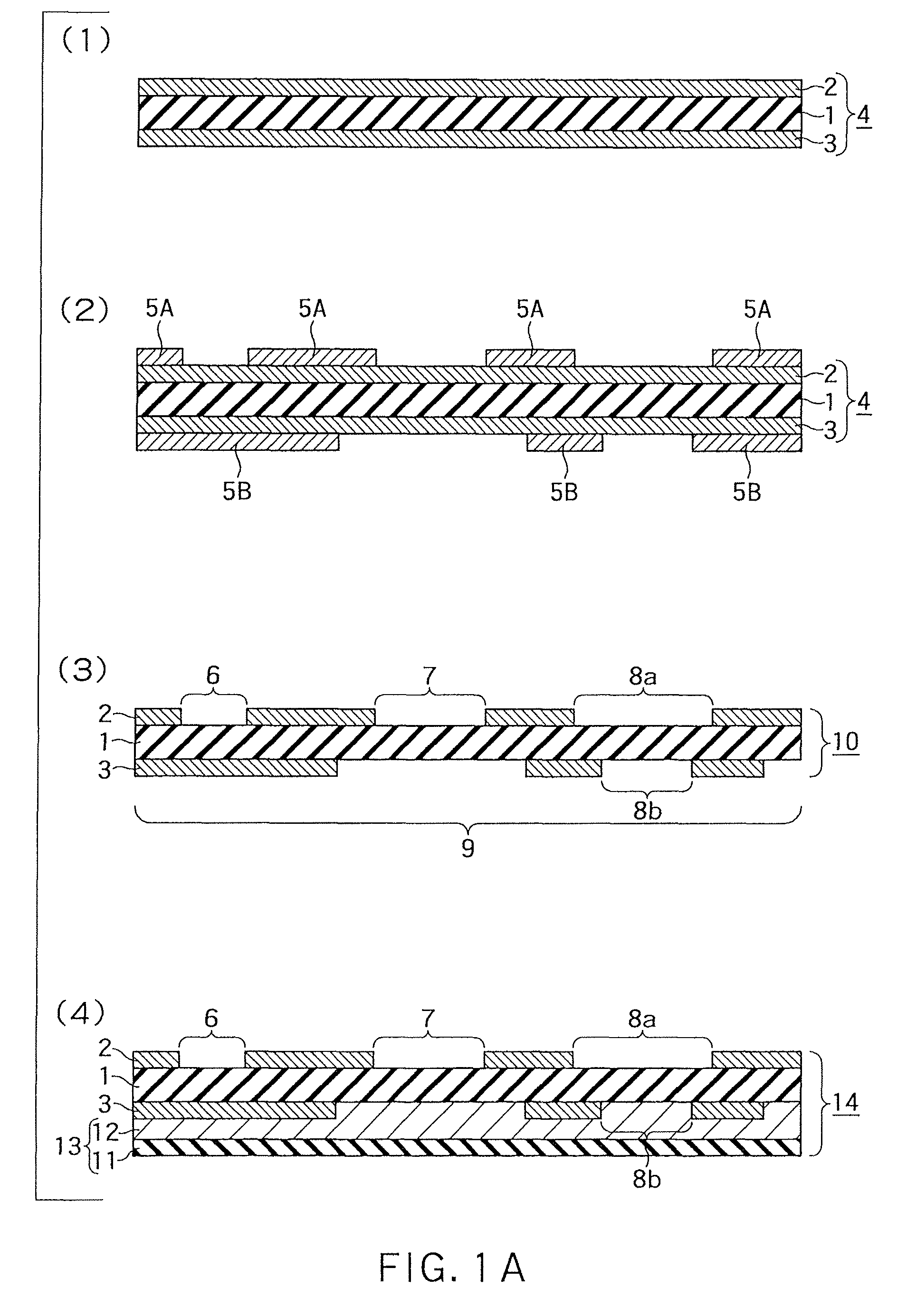
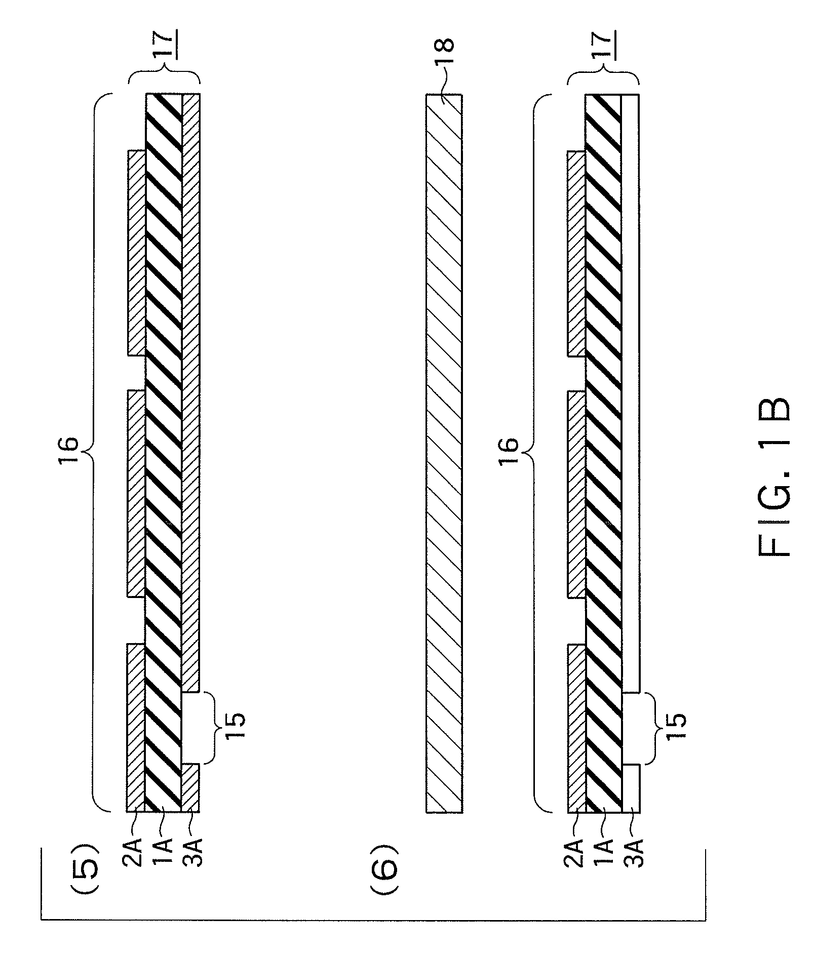
[0063]FIG. 1A to FIG. 1D are cross-sectional views illustrating a production method of a multilayer flexible printed wiring board according to Embodiment 1.

[0064](1) First, a flexible double-sided copper-clad laminate 4 is prepared. As illustrated in FIG. 1A(1), this double-sided copper-clad laminate 4 has copper foils 2 and 3 (each having a thickness of 12 μm, for example) on the both surfaces of a flexible insulating base member (first insulating layer) 1 (polyimide film having a thickness of 25 μm, for example). Here, the flexible insulating base member 1 is not limited to a film formed of polyimide, and it is possible to use a film formed of a liquid crystal polymer.

[0065]Also, the thicknesses of the flexible insulating base member 1, the copper foil 2 and the copper foil 3 are not limited to the above values and can be adequately selected depending on the intended use. For example, in a case where a high flexibility is required, it is preferable to select a thin thickness (for ...

example

[0098]Next, a result of actually investigating a relationship between the energy density of pulsed light of processing laser and a processing state of a via hole (i.e. step via hole 24) will be explained.

[0099]A configuration of the above multilayer circuit base material 19 (see FIG. 1C(7)) used in the present example is as follows.

[0100]Flexible insulating base member 1: Polyimide film having a thickness of 25 μm

[0101]Thickness of copper foils 2, 3, 2A and 3A: 12 μm

[0102]Flexible insulating film 11: Polyimide film having a thickness of 12 μm

[0103]Adhesive layers 12 and 18: Epoxy adhesive having a thickness of 15 μm

[0104]Diameter of mask hole 8a: 200 μm

[0105]Diameter of mask hole 8b: 150 μm

[0106]As a laser processing machine, ML605GTX (carbon dioxide laser) manufactured by in Mitsubishi Electric Corporation is used. The laser pulse with is fixed to 10 μsec and the laser beam radius is fixed to φ300 μm. Table 2 shows combinations (ID: 1 to 18) of the values of the first energy densit...

embodiment 2

[0135]Next, a production method of a multilayer flexible printed wiring board according to Embodiment 2 will be explained. One of differences between the present embodiment and Embodiment 1 is the number of processed layers at the time of forming a via hole. While the number of processed layers is four (i.e. the flexible insulating base member 1, the adhesive layer 12, the flexible insulating film 11 and the adhesive layer 18) in Embodiment 1, while the number of processed layers is two in the present embodiment.

[0136]FIG. 2A and FIG. 2B are process cross-sectional views illustrating the production method of the multilayer flexible printed wiring board according to Embodiment 2.

[0137](1) First, there is prepared a flexible one-surface copper-clad laminate having a copper foil 42 (for example, having a thickness of 12 μm) on one surface of a flexible insulating base material (first insulating layer) 41 (for example, polyimide film having a thickness of 25 μm). The flexible insulating...


PUM

PropertyMeasurementUnit
thicknessaaaaaaaaaa
thicknessaaaaaaaaaa
thicknessaaaaaaaaaa

Abstract

There is provided a laser processing method of forming via holes 23 and 24 by removing processed layers including a flexible insulating base member 1, in which conformal masks 7 and 8a are provided on the surface, and an adhesive layer 12 having a higher absorbance in a wavelength area of processing laser and a lower decomposition temperature than the insulating base member 1, the method including radiating one shot of pulse light having a first energy density that can remove the insulating base member 1 by one shot without causing the deformation and penetration of a conducting film 2A, and subsequently radiating pulse light having a second energy density that is lower than the first energy density and can remove the rest of the processed layers by a predetermined number of shots without causing the deformation and penetration of the conducting film 2A.

Description

CROSS-REFERENCE TO RELATED APPLICATIONS[0001]This is a national stage application of PCT / JP2011 / 051986 filed Feb. 1, 2011 and published in Japanese, which claims the priority of Japanese application number 2010-132922 filed Jun. 10, 2010, hereby incorporated by reference.BACKGROUND OF THE INVENTION[0002]1. Field of the Invention[0003]The present invention relates to a laser processing method and a production method of multilayer flexible printed wiring board using the laser processing method. Particularly, the present invention relates to a laser processing method of forming a via hole by removing multiple materials of different workability and a production method of multilayer flexible printed wiring board using the laser processing method.[0004]2. Background Art[0005]In recent years, as electronic devices are downsized and have higher functionality, there has been a growing demand for an increased density with respect to a printed wiring board. To realize a printed wiring board ca...

Claims


Application Information

Patent Timeline
Patent Type & Authority Patents(United States)
IPC IPC(8): H05K3/00B23K26/06H05K3/46H05K3/10B23K26/36B23K26/40H05K3/42B23K26/00B23K26/382
CPCH05K3/4685B23K26/063B23K26/367B23K26/409H05K3/0035H05K3/4635B23K2201/40H05K3/421H05K2203/108B23K26/364B23K26/0622B23K26/40B23K2103/172B23K2101/40
Inventor MATSUDA, FUMIHIKONARISAWA, YOSHIHIKO
Owner NIPPON MEKTRON LTD
Why Eureka
Try Eureka