Light confining devices using all-dielectric metamaterial cladding

a technology of dielectric metamaterials and confining devices, applied in the field of optical light confining devices, can solve the problems of reducing the propagation length, limiting the size of all conventional optical devices, and high power consumption, so as to reduce cross-talk, reduce the energy transfer between devices, and increase the spontaneous emission rate of an emitter

Active Publication Date: 2016-03-01
PURDUE RES FOUND INC
View PDF5 Cites 8 Cited by
  • Summary
  • Abstract
  • Description
  • Claims
  • Application Information

AI Technical Summary

Benefits of technology

[0008]The waveguides according to the invention include all-dielectric metamaterial claddings that can strongly confine light inside low-index dielectric waveguides. To design the metamaterial claddings, transforming optical momentum for controlling evanescent waves can be used. These transformations lead to a medium that supports total internal reflection and simultaneously makes the evanescent field outside the core of the waveguide decay faster. These transformations also lead to a class of metamaterials with dual electric and magnetic anisotropy and a very large birefringence which provides an ideal quasi-transverse electromagnetic mode propagation inside a glass core. Magnetism at the telecommunication wavelength is a challenge and strong confinement of the electric energy of a waveguide mode can be achieved with lossless semiconductor metamaterials. Transformed cladding waveguides with a permittivity, μij=1, and a permeability, ∈ij>1, provide an order of magnitude decreased cross-talk as compared to conventional waveguides making them suitable for multiple applications in dense photonic integration and nanophotonic devices.
[0009]An optical waveguide having a cladding composed of all-dielectric metamaterials is provided. In some embodiments, the diffraction limit of light can be surpassed by the use of a new class of metamaterials having a dielectric response that cannot be found in nature, but can be nanofabricated with readily available building blocks. These metamaterials do not have metallic building blocks thereby overcoming the shortcoming related to loss in the prior art. The rules of transformation optics can be used to transform optical momentum for controlling evanescent waves. With this class of transformations, it is possible to confine light inside a subwavelength low-index dielectric rod surrounded by metamaterial claddings. This transformation can cause the propagating mode to become close to a transverse electromagnetic (TEM) mode. In some embodiments, a practically achievable all-dielectric metamaterial waveguide can be shown with reduced mode area and increased power confinement in the core for use in dense photonic integration. In some embodiments, the metamaterial waveguide can dramatically decrease crosstalk between two slab waveguides at infrared wavelengths and, in some embodiments, at the telecommunication optical wavelength (i.e. 1550 nm).
[0023]An optical waveguide for use with electromagnetic signals operating at infrared wavelengths is provided, the optical waveguide including a core that is substantially transparent at the infrared wavelengths, the core having a longitudinal axis, z, and orthogonal axes, x and y, that are substantially perpendicular to the longitudinal axis, the core further having a radius in a plane defined by the x and y axes that is a fraction of the infrared wavelengths; and a metamaterial cladding disposed around the core, the cladding anisotropy configured to provide total internal reflection and also increase the decay of evanescent waves, the waveguide providing quasi-transverse electromagnetic mode propagation of the electromagnetic signals along the z axis of the core, provide sub-diffraction confinement of light without loss and strong confinement of light inside the core using metamaterial anisotropy. The core may include silica or silicon. The core may have a cross-section shape that is one or more from a group consisting of circular, square, rectangular, slab, slot, strip and rib.
[0024]The cladding may include a homogeneous lossless anisotropic metamaterial. The cladding may have alternating thin film layers of a high index semiconductor and a second low index cladding material, wherein each layer of high index semiconductor and the second cladding material has a width that is a fraction of the infrared wavelengths. The high index semiconductor may be Germanium or Silicon. The second cladding material may include one or more from a group consisting of air, silica, porous silica and silicon. A photonic integrated device may include at least one optical waveguide as set forth above and may use anisotropy to increase decay of evanescent waves.
[0027]An electromagnetic wave confining device is provided that has anisotropic dielectric constants in the cladding providing total internal reflection and fast decay of evanescent waves and provides reduced cross-talk between adjacent devices.
[0030]A light confining device with a core surrounded by anisotropic metamaterial cladding is provided which uses no metallic components; causes no absorption losses in the metamaterial; provides reduced cross-talk between adjacent waveguides for photonic integration; confines light as a resonator below the diffraction limit for active devices; provides reduction in energy transfer between devices if the core of the waveguides are active; provides increase in the spontaneous emission rate of an emitter if placed inside the core; and provides enhanced nonlinearity if the core is non-linear.

Problems solved by technology

Light has a characteristic size, the wavelength, which sets a limit to all conventional optical device sizes, especially waveguides and resonators.
Coupling light to free electrons of metals leads to plasmonic waveguides that can overcome this limitation, but their high optical losses cause a reduced propagation length and high power consumption, a major impediment for integrated photonic circuits.
Relying on optical waveguides as interconnects can increase the speed as well as functionality of integrated circuits, however, the diffraction limit of light is a fundamental barrier to interface micron scale waveguides to nanoscale electronic circuitry.
Furthermore, dense photonic integration is hampered because crosstalk between waveguides increases as the separation between them is reduced.
V-groove and wedge plasmon are an excellent candidates for relatively long range propagation and sub-diffraction confinement, however excitation and detection of these modes as well as interfacing with existing silicon waveguide technology are a major challenge.
However, due to absorption in metals, the above mentioned sub-diffraction plasmonic structures cannot guide light more than a few microns.
Furthermore, the dissipated energy leads to thermal issues which are especially significant in miniaturized circuits hindering dense photonic integration.

Method used


Image

  • Light confining devices using all-dielectric metamaterial cladding
  • Light confining devices using all-dielectric metamaterial cladding
  • Light confining devices using all-dielectric metamaterial cladding

Examples


Embodiment Construction

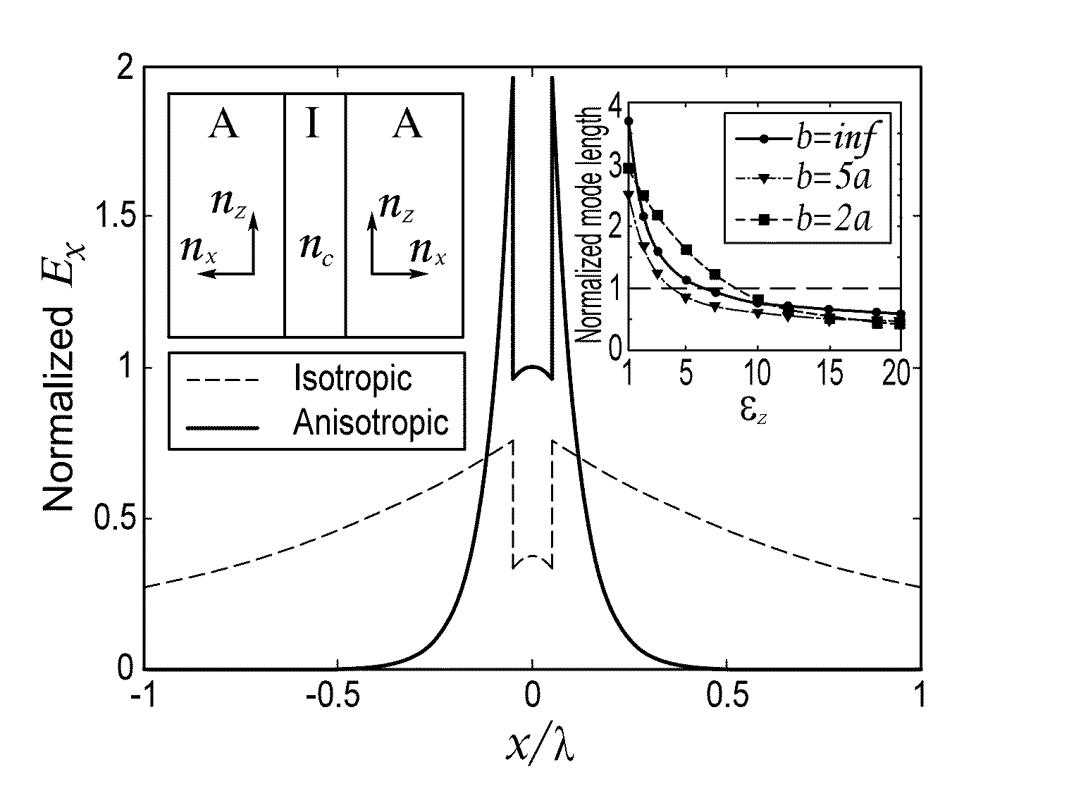
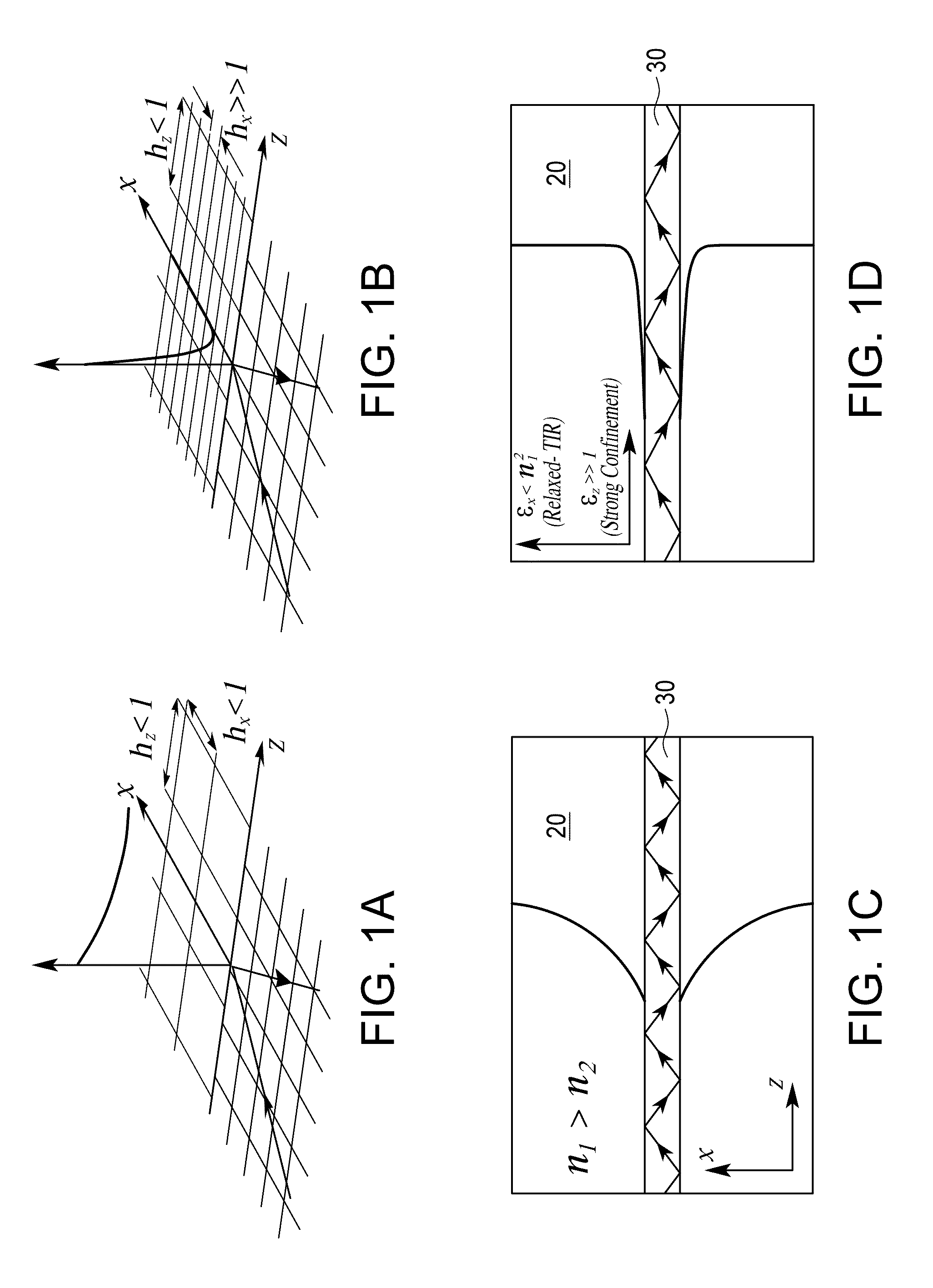
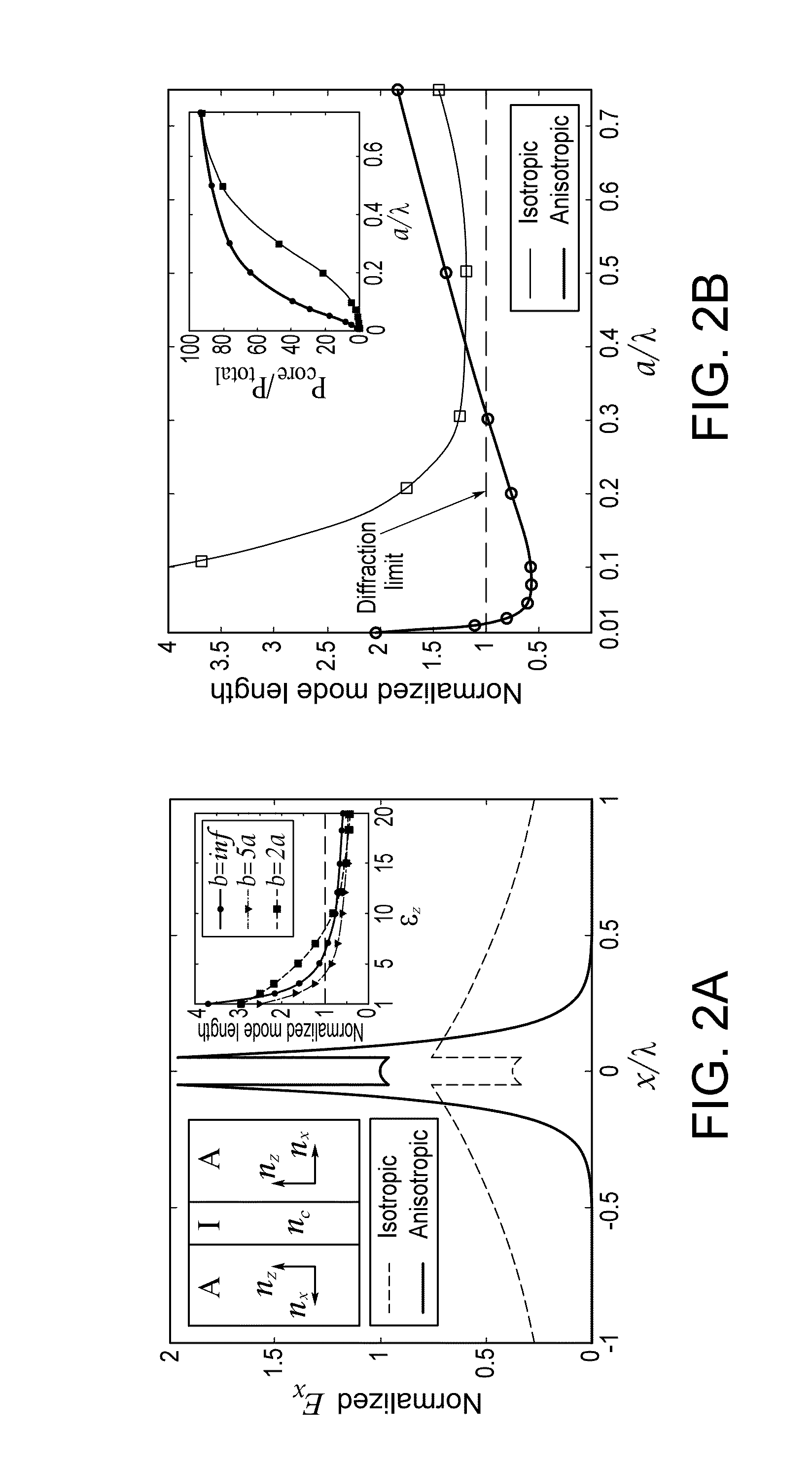
[0038]An optical waveguide having a cladding composed of all-dielectric metamaterials is provided.

[0039]All-dielectric waveguides are useful for low-loss confinement of electromagnetic waves at optical frequencies, e.g. slot waveguides and photonic crystal waveguides. Slot waveguides can confine and enhance the electric field inside a sub-diffraction low-index dielectric slot between high index waveguides, which is suitable for many applications, such as nonlinear and quantum optics. The enhancement in the slot arises due to the continuity condition on the displacement vector at the low-index / high-index interface. However, most of the power lies outside the slot region and decays slowly. Thus, the slot waveguide performance in a dense Photonic Integrated Circuit (“PIC”) is not comparable to a conventional rod waveguide due to crosstalk.

[0040]The light confinement mechanism in Photonic crystal (“PhC”) waveguides is the bragg reflection of waves in the bandgap of the PhC. The properti...


PUM


Abstract

An all-dielectric metamaterial cladding is provided that can strongly confine light inside conventional low-index dielectric waveguides for use with photonic integrated circuits and nano-photonic devices. A class of metamaterials with dual electric and magnetic anisotropy along with giant birefringence can provide the ideal quasi-transverse electromagnetic mode propagation inside a glass core. A Transformed Cladding Waveguide can show an order of magnitude decreased cross-talk as compared to conventional waveguides.

Description

[0001]This application claims the benefit of U.S. Provisional Patent Application Ser. No. 61 / 762,146, filed Feb. 7, 2013, which is hereby incorporated by reference in its entirety.FIELD OF THE INVENTION[0002]The present disclosure is related to the field of optical light confining devices such as resonators and waveguides, and more particularly to optical waveguides for use in integrated photonic circuits.BACKGROUND OF THE INVENTION[0003]Light has a characteristic size, the wavelength, which sets a limit to all conventional optical device sizes, especially waveguides and resonators. This limit called the diffraction limit is a fundamental obstacle and is defined as the size of the optical mode in a resonator or waveguide. The value is given by (λ / 2ncore)^3 in a 3D geometry, (λ / 2ncore)^2 in a 2D geometry and (λ / 2ncore)^1 in a 1D geometry. Here, λ / 2ncore is the wavelength in free space divided by twice the value of the refractive index of the core of the waveguide or resonator. The ab...

Claims


Application Information

Patent Timeline
Patent Type & Authority Patents(United States)
IPC IPC(8): G02B6/12G02B6/122G02B27/01G02B1/00G02B6/02B82Y20/00
CPCG02B6/1225G02B1/002G02B6/023G02B6/0229G02B6/02295G02B27/0176B82Y20/00G02B2006/12035G02B2006/12061Y10S977/932
Inventor JAHANI, SAMANJACOB, ZUBIN
Owner PURDUE RES FOUND INC
Why Eureka
Try Eureka