
Light confining devices using all-dielectric metamaterial cladding

a technology of dielectric metamaterials and confining devices, applied in the field of optical light confining devices, can solve the problems of reducing the propagation length, limiting the size of all conventional optical devices, and high power consumption, so as to reduce cross-talk, reduce the energy transfer between devices, and increase the spontaneous emission rate of an emitter

Active Publication Date: 2014-12-04
PURDUE RES FOUND INC
View PDF5 Cites 7 Cited by
  • Summary
  • Abstract
  • Description
  • Claims
  • Application Information

AI Technical Summary

Benefits of technology

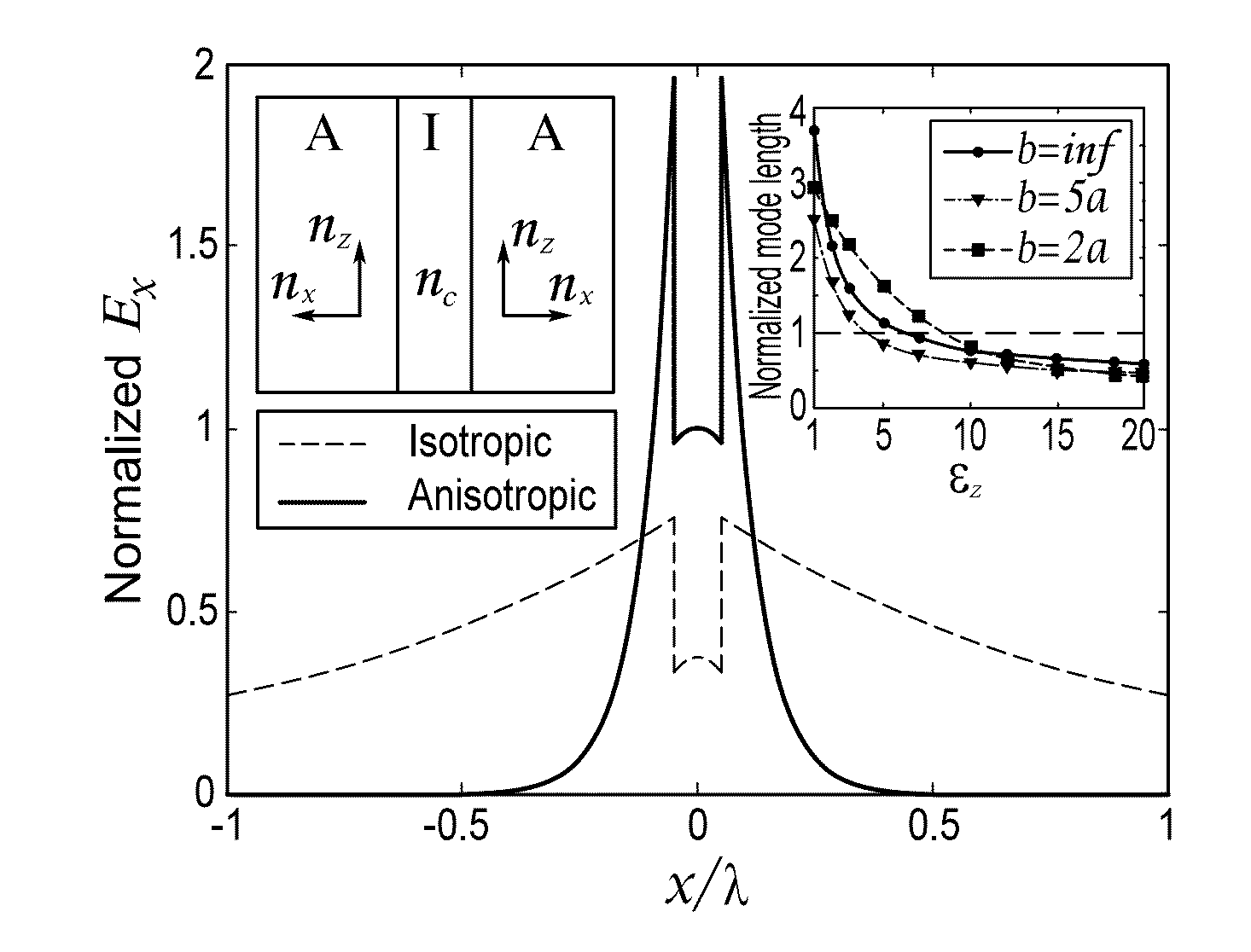
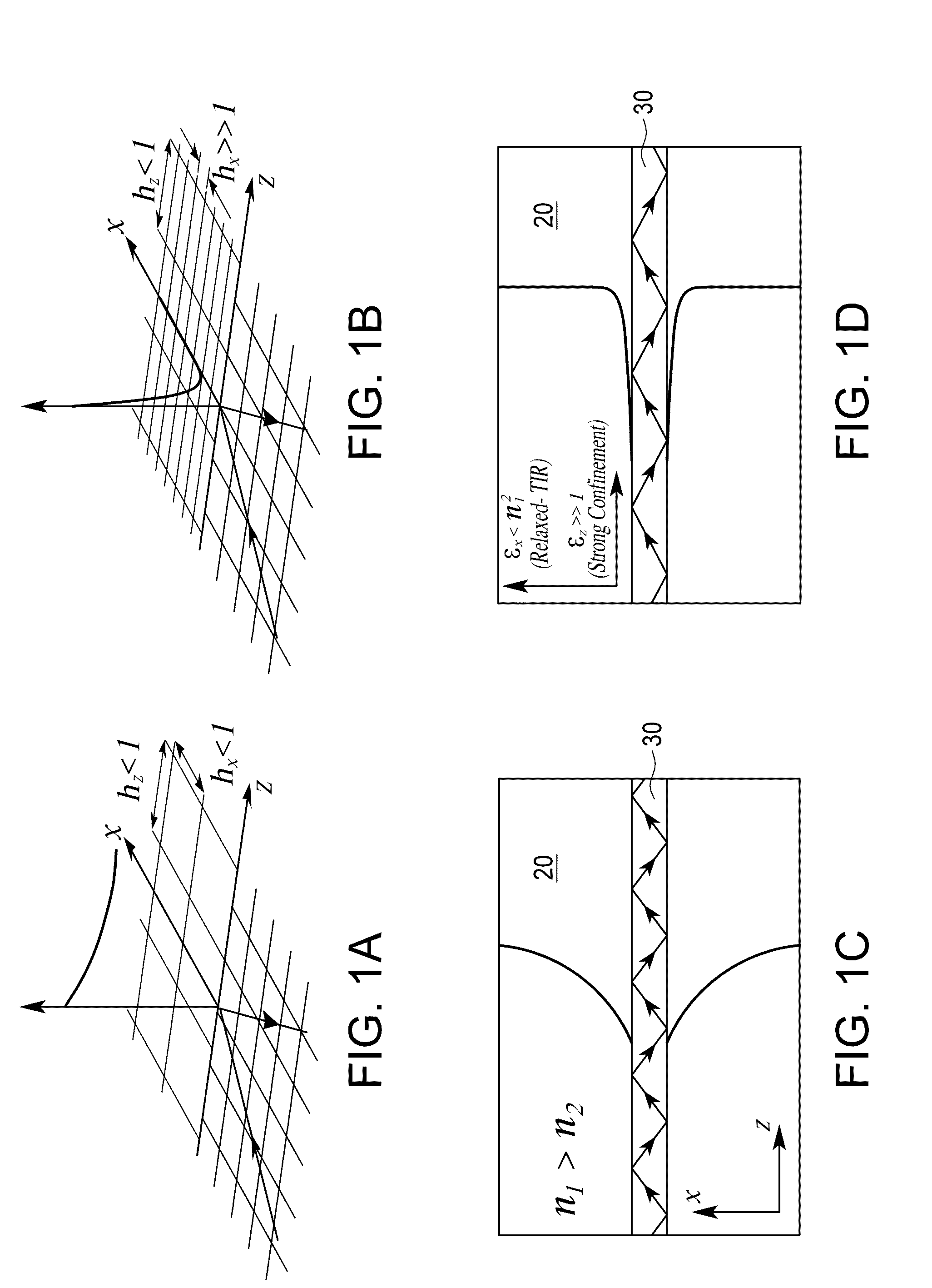
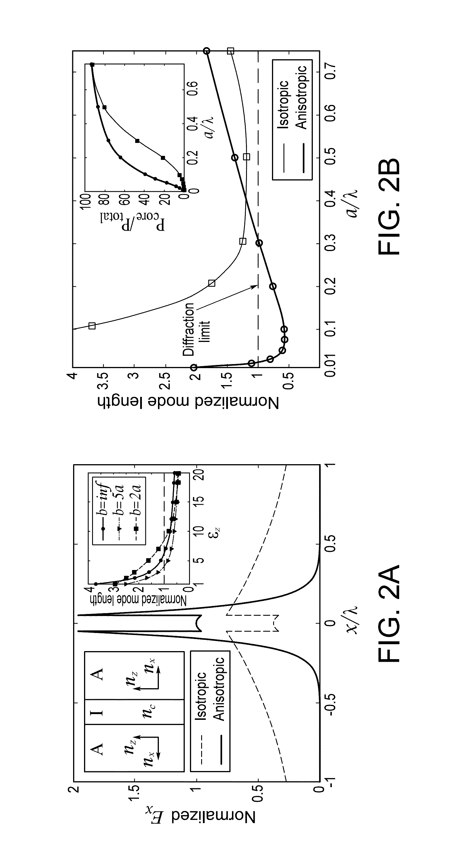
The invention is about waveguides that use all-dielectric metamaterial claddings to confine light inside low-index dielectric waveguides. These claddings can strongly confine light inside the waveguide, reducing cross-talk between neighboring waveguides. The metamaterial claddings have dual electric and magnetic anisotropy, which makes them ideal for use in dense photonic integration and nanophotonic devices. The waveguides can be designed to have a reduced mode area and increased power confinement in the core, and can be used for optical communication at infrared wavelengths. The invention provides a way to overcome the limitations of conventional waveguides and offers improved performance for optical devices.

Problems solved by technology

Light has a characteristic size, the wavelength, which sets a limit to all conventional optical device sizes, especially waveguides and resonators.
Coupling light to free electrons of metals leads to plasmonic waveguides that can overcome this limitation, but their high optical losses cause a reduced propagation length and high power consumption, a major impediment for integrated photonic circuits.
Relying on optical waveguides as interconnects can increase the speed as well as functionality of integrated circuits, however, the diffraction limit of light is a fundamental barrier to interface micron scale waveguides to nanoscale electronic circuitry.
Furthermore, dense photonic integration is hampered because crosstalk between waveguides increases as the separation between them is reduced.
V-groove and wedge plasmon are an excellent candidates for relatively long range propagation and sub-diffraction confinement, however excitation and detection of these modes as well as interfacing with existing silicon waveguide technology are a major challenge.
However, due to absorption in metals, the above mentioned sub-diffraction plasmonic structures cannot guide light more than a few microns.
Furthermore, the dissipated energy leads to thermal issues which are especially significant in miniaturized circuits hindering dense photonic integration.

Method used


Image

  • Light confining devices using all-dielectric metamaterial cladding
  • Light confining devices using all-dielectric metamaterial cladding
  • Light confining devices using all-dielectric metamaterial cladding

Examples


Embodiment Construction

[0039]An optical waveguide having a cladding composed of all-dielectric metamaterials is provided.

[0040]All-dielectric waveguides are useful for low-loss confinement of electromagnetic waves at optical frequencies, e.g. slot waveguides and photonic crystal waveguides. Slot waveguides can confine and enhance the electric field inside a sub-diffraction low-index dielectric slot between high index waveguides, which is suitable for many applications, such as nonlinear and quantum optics. The enhancement in the slot arises due to the continuity condition on the displacement vector at the low-index / high-index interface. However, most of the power lies outside the slot region and decays slowly. Thus, the slot waveguide performance in a dense Photonic Integrated Circuit (“PIC”) is not comparable to a conventional rod waveguide due to crosstalk.

[0041]The light confinement mechanism in Photonic crystal (“PhC”) waveguides is the bragg reflection of waves in the bandgap of the PhC. The properti...


PUM


Abstract

An all-dielectric metamaterial cladding is provided that can strongly confine light inside conventional low-index dielectric waveguides for use with photonic integrated circuits and nano-photonic devices. A class of metamaterials with dual electric and magnetic anisotropy along with giant birefringence can provide the ideal quasi-transverse electromagnetic mode propagation inside a glass core. A Transformed Cladding Waveguide can show an order of magnitude decreased cross-talk as compared to conventional waveguides.

Description

[0001]This application claims the benefit of U.S. Provisional Patent Application Ser. No. 61 / 762,146, filed Feb. 7, 2013, which is hereby incorporated by reference in its entirety.FIELD OF THE INVENTION[0002]The present disclosure is related to the field of optical light confining devices such as resonators and waveguides, and more particularly to optical waveguides for use in integrated photonic circuits.BACKGROUND OF THE INVENTION[0003]Light has a characteristic size, the wavelength, which sets a limit to all conventional optical device sizes, especially waveguides and resonators. This limit called the diffraction limit is a fundamental obstacle and is defined as the size of the optical mode in a resonator or waveguide. The value is given by (λ / 2ncore)̂3 in a 3D geometry, (λ / 2ncore)̂2 in a 2D geometry and (λ / 2ncore)̂1 in a 1D geometry. Here, λ / 2ncore is the wavelength in free space divided by twice the value of the refractive index of the core of the waveguide or resonator. The ab...

Claims


Application Information

Patent Timeline
IPC IPC(8): G02B6/122G02B1/00G02B6/02
CPCG02B6/1225G02B6/02295G02B1/002G02B6/023Y10S977/932G02B2006/12035G02B2006/12061B82Y20/00G02B6/0229G02B27/0176
Inventor JAHANI, SAMANJACOB, ZUBIN
Owner PURDUE RES FOUND INC
Learn More