Silicon carbide MOSFET with integrated MOS diode

a technology of silicon carbide mosfet and diode, which is applied in the direction of diodes, semiconductor devices, electrical apparatus, etc., can solve the problems of high conduction loss, diodes also have a significant amount of stored charge, and suffer from three major limitations in practice, so as to improve low field mobility, reduce the threshold voltage, and reduce the effect of knee voltag

Active Publication Date: 2016-04-26
UNITED SILICON CARBIDE
View PDF9 Cites 15 Cited by
  • Summary
  • Abstract
  • Description
  • Claims
  • Application Information

AI Technical Summary

Benefits of technology

[0006]The threshold voltage of the MOS diode can be used to develop a lower knee voltage. The threshold of the MOS diode can be substantially smaller than that of the MOSFET. The MOS diode may be implemented with channel mobility enhancement materials and / or higher dielectric constant gate materials. The MOS diode may have a very thin gate dielectric. The MOS diode channel base may be implanted with a material such as nitrogen, antimony, and / or arsenic to obtain better low field mobility. The MOS diode channel base may also be implanted with a higher level of dopant than the MOSFET channel base. The MOSFET gate conductor and MOS diode gate conductor may be made of polysilicon doped with opposite dopant types. The MOS diode gate dielectric may be implanted with cesium or other ions to produce a positive oxide charge in order to reduce its threshold voltage.

Problems solved by technology

However, this practice suffers from three major limitations.
The body diode has a high knee voltage before the onset of conduction, leading to high conduction losses.
The body diode also has a significant amount of stored charge which increases with temperature, removal of which leads to turn-on losses in adjacent devices.
Finally, if the body diode is allowed to conduct, the recombination that occurs in electron-hole plasma in the device may result in progressive device degradation by causing an expansion of basal plane defects in the crystal in the case of SiC.
This degradation manifests as an increase in leakage current and on-state voltage drop, causing the devices to dissipate more in losses as they age, and can eventually lead to catastrophic destruction.
However, integrating a JBS diode limits the knee voltage based on the Schottky diode barrier height.

Method used


Image

  • Silicon carbide MOSFET with integrated MOS diode
  • Silicon carbide MOSFET with integrated MOS diode
  • Silicon carbide MOSFET with integrated MOS diode

Examples


examples

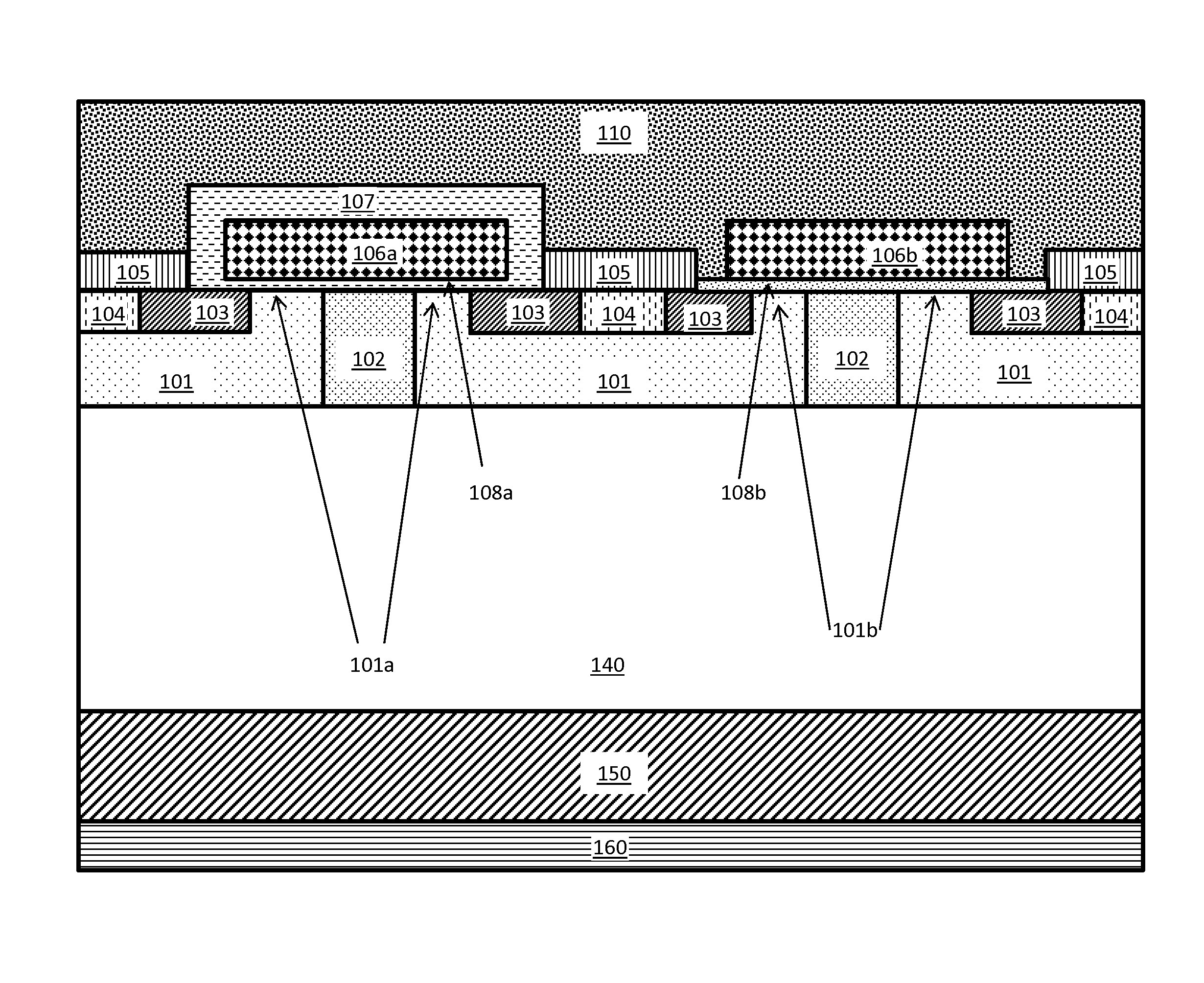
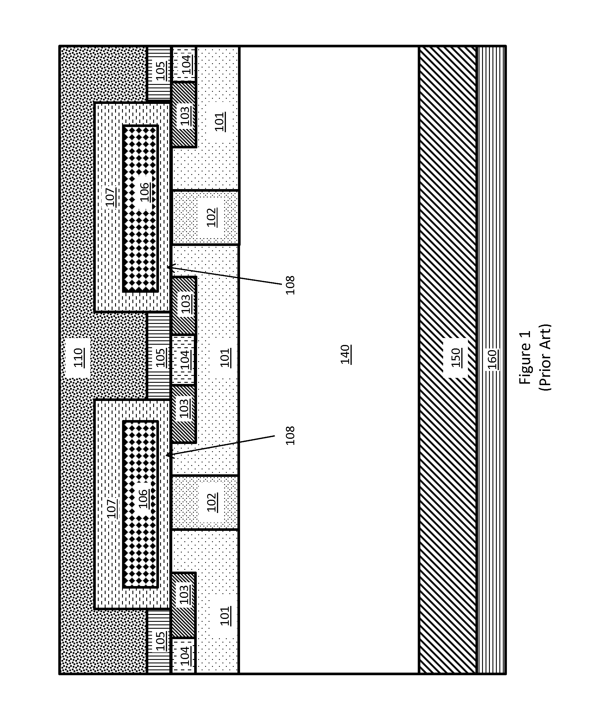
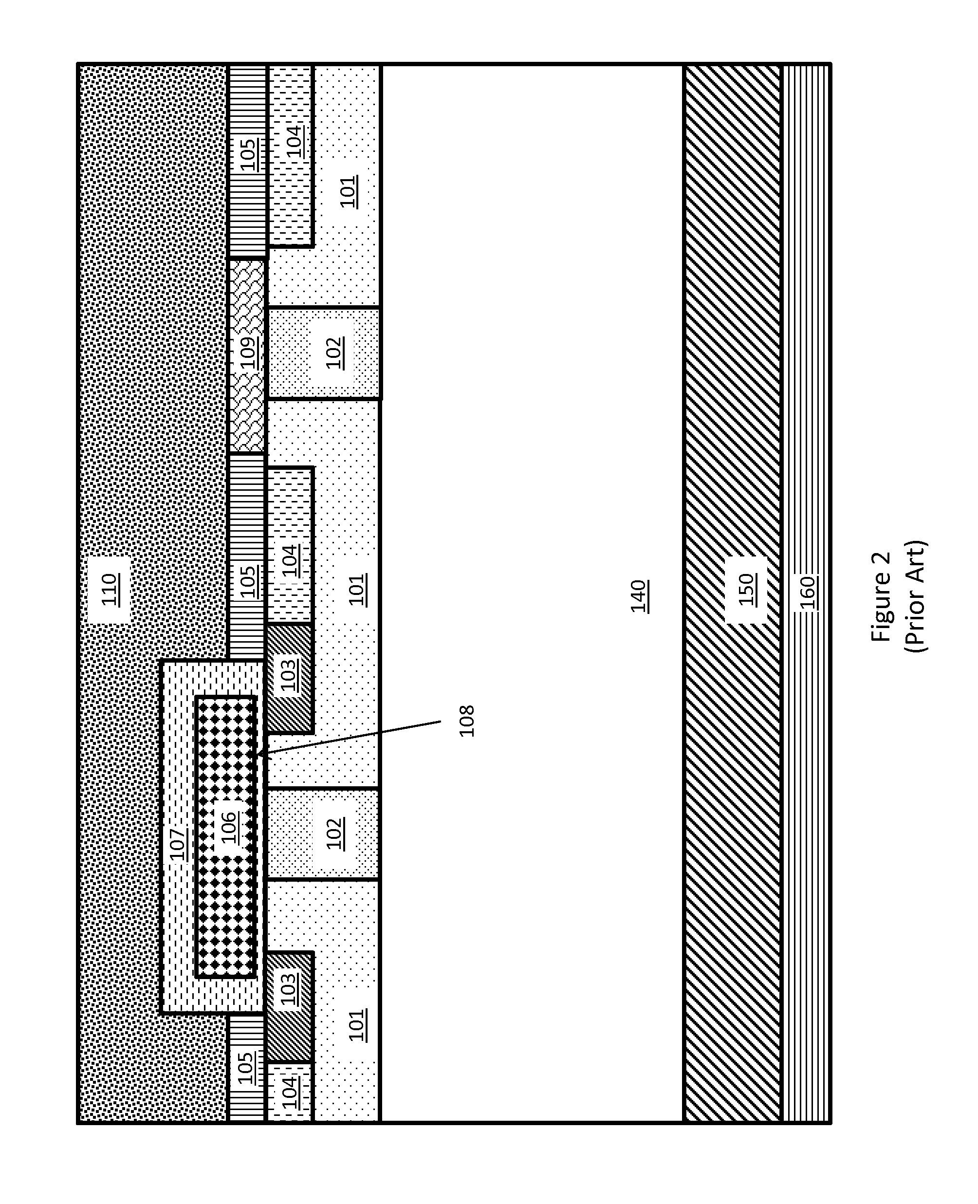
[0039]A compound semiconductor device may include a MOSFET monolithically integrated with a MOS diode. The MOSFET and MOS diode may be formed on the same substrate using identical or analogous process steps. An n-MOSFET may include an n-doped drift and an n-doped source, a p-doped channel base, a gate conductor, and a gate oxide, with the drift connected to an n-doped substrate drain. An n-MOS diode paired with the MOSFET may share the same substrate drain and drift region. Similarly, the MOS diode gate conductor and channel base may be formed at the same time as the analogous structures for the MOSFET. The MOS diode is formed by connecting the MOS diode gate conductor to both the diode source and the MOSFET source. The MOSFET and the MOS diode may both be made of silicon carbide, gallium nitride, aluminum nitride, aluminum gallium nitride, diamond, or other semiconductor material.

[0040]Compound devices pairing a MOSFET and a MOS diode can be achieved in a number of configurations i...


PUM

PropertyMeasurementUnit
threshold voltageaaaaaaaaaa
thicknessaaaaaaaaaa

Abstract

A monolithically integrated MOS channel in gate-source shorted mode is used as a diode for the third quadrant conduction path for a power MOSFET. The MOS diode and MOSFET can be constructed in a variety of configurations including split-cell and trench. The devices may be formed of silicon carbide, gallium nitride, aluminum nitride, aluminum gallium nitride, diamond, or similar semiconductor. Low storage capacitance and low knee voltage for the MOS diode can be achieved by a variety of means. The MOS diode may be implemented with channel mobility enhancement materials, and/or have a very thin/high permittivity gate dielectric. The MOSFET gate conductor and MOS diode gate conductor may be made of polysilicon doped with opposite dopant types. The surface of the MOS diode dielectric may be implanted with cesium.

Description

FIELD OF THE DISCLOSURE[0001]This disclosure is in the field of high-current and high-voltage metal oxide field effect transistors (MOSFETs) made from such materials as silicon carbide (SiC), gallium nitride (GaN), aluminum nitride (AlN), aluminum gallium nitride (AlGaN), and diamond. MOSFETs with integrated diodes and methods of making the same are disclosed.BACKGROUND[0002]High-current and high voltage MOSFETs with integrated diodes made from SiC, GaN, and other materials are useful in power electronic circuits, such as power factor correction (PFC) devices, DC-DC converters, DC-AC inverters, overcurrent and overvoltage protection circuits, and motor drives.[0003]In many prior art SiC and GaN MOSFETs used in power electronic circuits, for example, the built-in body diode is used to carry the third quadrant / freewheeling current. However, this practice suffers from three major limitations. The body diode has a high knee voltage before the onset of conduction, leading to high conduct...

Claims


Application Information

Patent Timeline
Patent Type & Authority Patents(United States)
IPC IPC(8): H01L29/16H01L29/10H01L27/06H01L29/739H01L29/78H01L29/40H01L29/423H01L29/51H01L29/49H01L29/167
CPCH01L29/7803H01L29/1608H01L29/7813H01L29/7391H01L27/0629H01L29/42364H01L29/7828H01L29/861H01L29/1602H01L29/2003H01L29/1095H01L29/4916H01L29/51H01L29/42312H01L29/407
Inventor BHALLA, ANUPFURSIN, LEONID
Owner UNITED SILICON CARBIDE
Why Eureka
Try Eureka