
Method of endpoint detection of plasma etching process using multivariate analysis

a plasma etching and multi-variate analysis technology, applied in semiconductor/solid-state device testing/measurement, instruments, electric discharge tubes, etc., can solve the problem of not normalizing the data of optical emission spectroscopy (oes), and achieve the effect of improving the data quality for further processing and removing nois

Active Publication Date: 2016-05-03
TOKYO ELECTRON LTD
View PDF11 Cites 8 Cited by
  • Summary
  • Abstract
  • Description
  • Claims
  • Application Information

AI Technical Summary

Benefits of technology

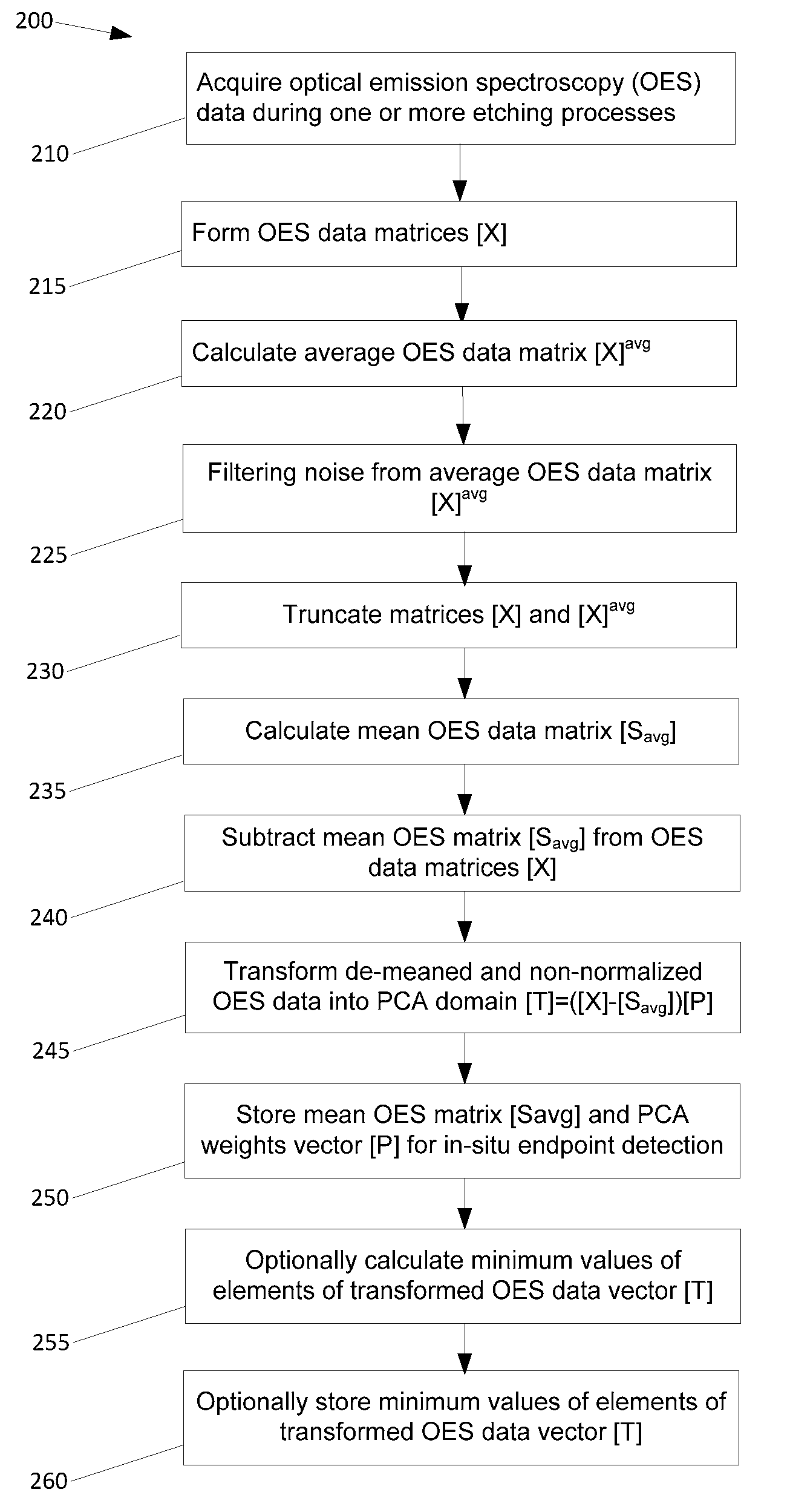
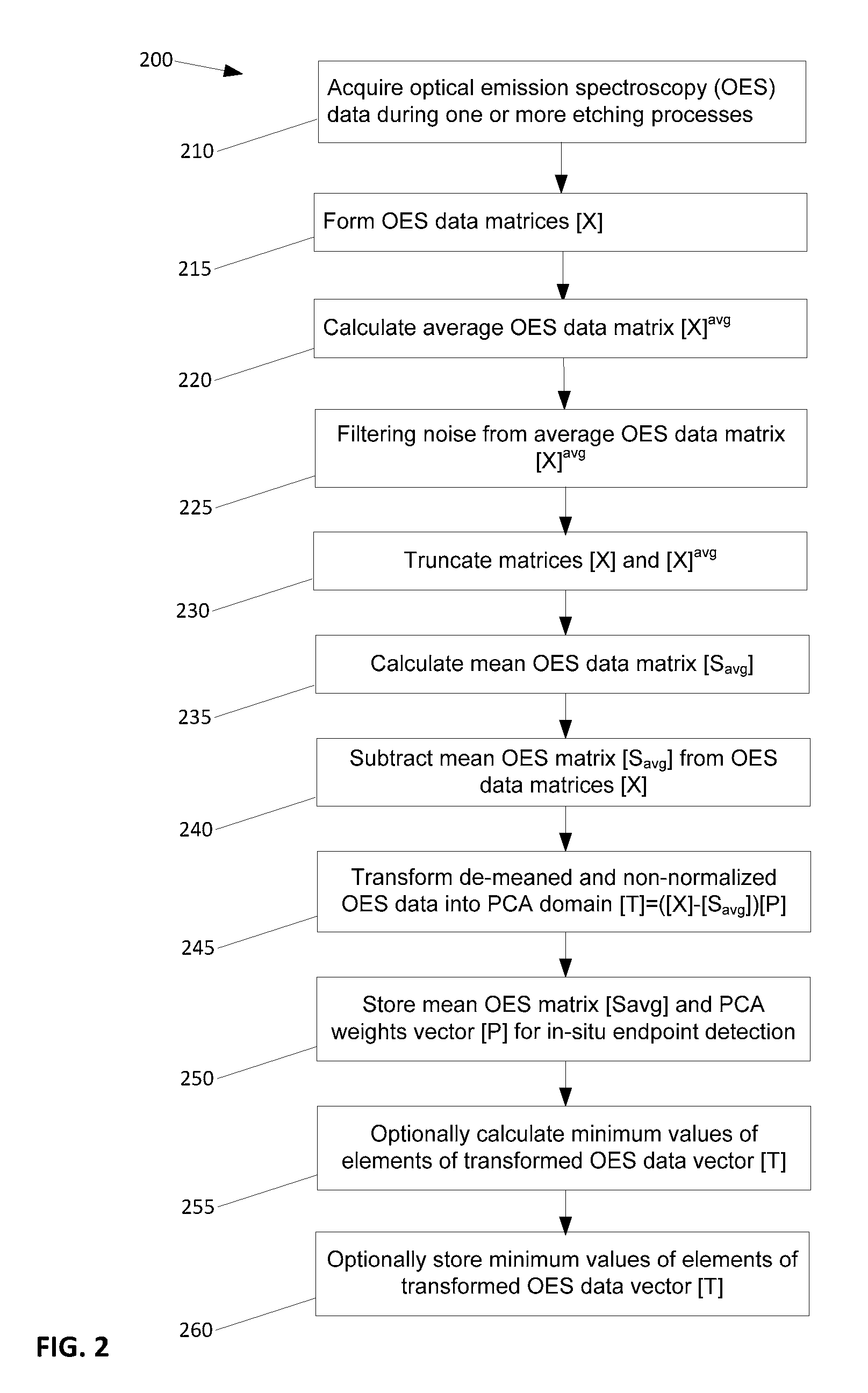
The patent describes a method for improving the quality of optical emission spectroscopy (OES) data collected during a plasma etch process. The data is acquired and then averaged to remove noise. However, the data is not normalized before being used for further analysis. A mean OES data matrix is then calculated by subtracting the average from the original data matrices. This results in a de-meanned OES data set, which can be utilized for further analysis, such as multivariate analysis. The technical effect of this method is the improvement of data quality for OES analysis during plasma etch processes.

Problems solved by technology

However, unlike what is usually done in multivariate analysis, the optical emission spectroscopy (OES) data is not normalized prior to being used as input for multivariate analysis.

Method used


Image

  • Method of endpoint detection of plasma etching process using multivariate analysis
  • Method of endpoint detection of plasma etching process using multivariate analysis
  • Method of endpoint detection of plasma etching process using multivariate analysis

Examples


Embodiment Construction

[0021]In the following description, in order to facilitate a thorough understanding of the invention and for purposes of explanation and not limitation, specific details are set forth, such as particular geometries of a lithography, coater / developer, and gap-fill treatment system, and descriptions of various components and processes. However, it should be understood that the invention may be practiced in other embodiments that depart from these specific details.

[0022]In the description to follow, the terms radiation-sensitive material and photoresist may be used interchangeably, photoresist being only one of many suitable radiation-sensitive materials for use in photolithography. Similarly, hereinafter the term substrate, which represents the workpiece being processed, may be used interchangeably with terms such as semiconductor wafer, LCD panel, light-emitting diode (LED), photovoltaic (PV) device panel, etc., the processing of all of which falls within the scope of the claimed inv...


PUM

PropertyMeasurementUnit
pressuresaaaaaaaaaa
pressureaaaaaaaaaa
frequencyaaaaaaaaaa

Abstract

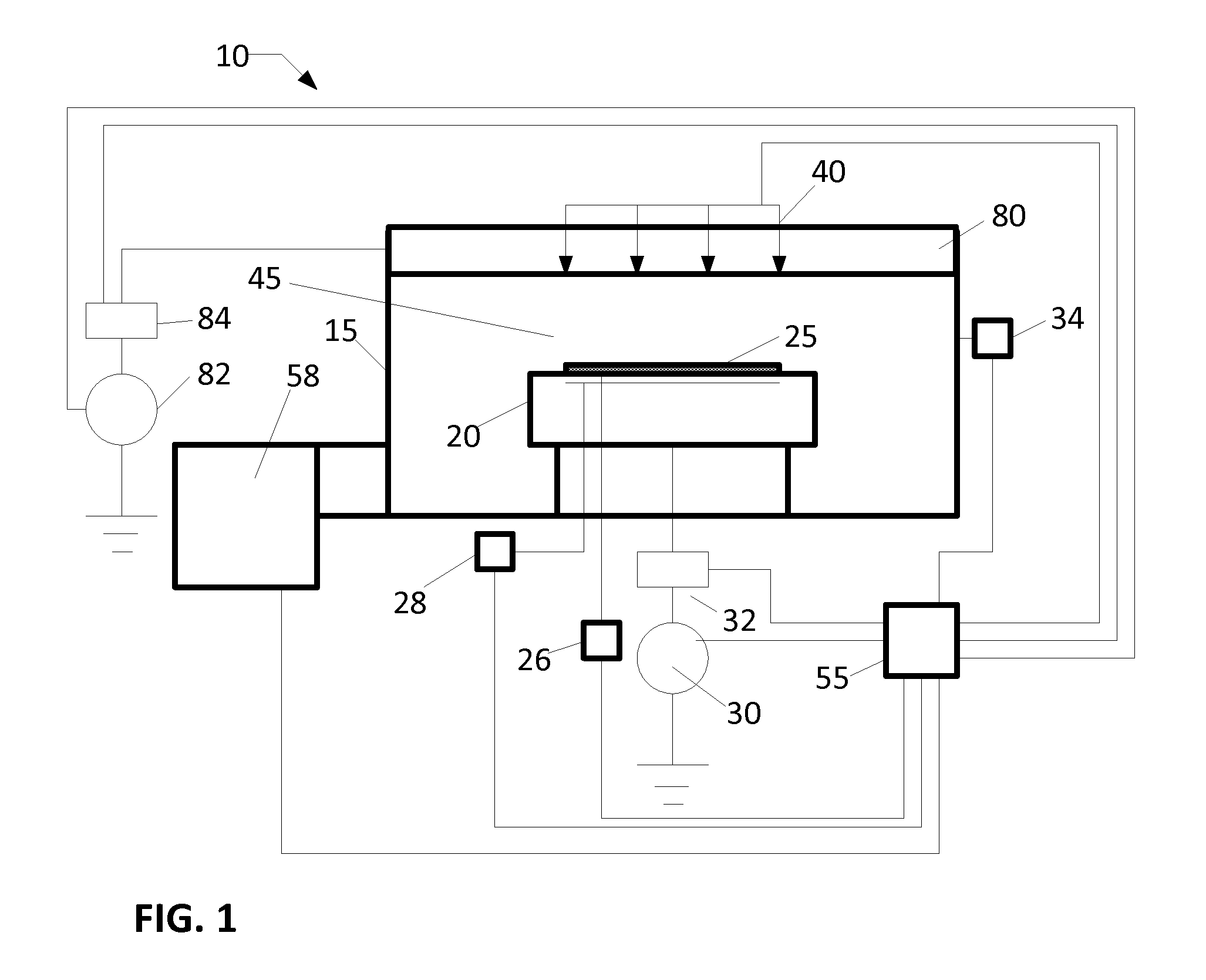
Disclosed is a method for determining an endpoint of an etch process using optical emission spectroscopy (OES) data as an input. Optical emission spectroscopy (OES) data are acquired by a spectrometer attached to a plasma etch processing tool. The acquired time-evolving spectral data are first filtered and demeaned, and thereafter transformed into transformed spectral data, or trends, using multivariate analysis such as principal components analysis, in which previously calculated principal component weights are used to accomplish the transform. A functional form incorporating multiple trends may be used to more precisely determine the endpoint of an etch process. A method for calculating principal component weights prior to actual etching, based on OES data collected from previous etch processing, is disclosed, which method facilitates rapid calculation of trends and functional forms involving multiple trends, for efficient and accurate in-line determination of etch process endpoint.

Description

CROSS REFERENCE TO RELATED APPLICATIONS[0001]This application is based on and claims the benefit of and priority to U.S. Provisional Patent Application No. 61 / 715,047, entitled “METHOD OF ENDPOINT DETECTION OF PLASMA ETCHING PROCESS USING MULTIVARIATE ANALYSIS”, filed on Oct. 17, 2012, the entire contents of which are herein incorporated by reference.BACKGROUND OF THE INVENTION[0002]1. Field of the Invention[0003]The present invention relates to a method and system for controlling the process of etching a structure on a substrate, for example, in semiconductor manufacturing. More particularly, it relates to a method for determining an endpoint of an etch process.[0004]2. Description of Related Art[0005]Plasma etch processes are commonly used in conjunction with photolithography in the process of manufacturing semiconductor devices, liquid crystal displays (LCDs), light-emitting diodes (LEDs), and some photovoltaics (PVs). Generally, a layer of radiation-sensitive material, such as p...

Claims


Application Information

Patent Timeline
Patent Type & Authority Patents(United States)
IPC IPC(8): G01L21/30H01J37/32H01L21/66G01R31/00G06F17/16H01L21/67
CPCH01L22/26G06F17/16H01J37/32963H01L21/67069H01L21/3065
Inventor CHEN, YANKOMAROV, SERGUEIVUONG, VI
Owner TOKYO ELECTRON LTD
Learn More