Back gate bias voltage control of oxide semiconductor transistor

a technology of back gate bias and oxide semiconductor, which is applied in the field of semiconductor devices, can solve the problems of difficult control of the threshold voltage of an oxide semiconductor transistor, variations in the characteristics of transistors, and the threshold voltage of a transistor change, so as to achieve stable control, reduce power consumption, and high speed operation

Active Publication Date: 2016-06-28
SEMICON ENERGY LAB CO LTD
View PDF143 Cites 5 Cited by
  • Summary
  • Abstract
  • Description
  • Claims
  • Application Information

AI Technical Summary

Benefits of technology

[0008]Another object of the present invention is to provide a semiconductor device having a stable threshold voltage of an oxide semiconductor transistor even when a usage environment of the semiconductor device, e.g., temperature, is changed. Another object of the present invention is to provide a semiconductor device having a stable threshold voltage of an oxide semiconductor transistor even when a variation in transistor characteristics occurs in a manufacturing process. Another object of the present invention is to provide a semiconductor device in which an off-state current can be controlled stably.
[0014]By the control operation of the present invention, a semiconductor device in which a shift in the threshold voltage of an oxide semiconductor transistor caused by temperature or a variation in transistor characteristics is less likely to occur can be provided. A semiconductor device in which an off-state current of an oxide semiconductor transistor can be stably controlled without being affected by temperature or a variation in transistor characteristics can be provided.
[0015]A memory device or a semiconductor device with less power consumption can be provided. A memory device or a semiconductor device capable of high speed operation can be provided.

Problems solved by technology

On the other hand, controlling a threshold voltage of an oxide semiconductor transistor is difficult.
However, in the case where a back gate voltage is fixed, a problem of variations in transistor characteristics or a change in threshold voltages of transistors caused by temperature characteristics occurs.

Method used


Image

  • Back gate bias voltage control of oxide semiconductor transistor
  • Back gate bias voltage control of oxide semiconductor transistor
  • Back gate bias voltage control of oxide semiconductor transistor

Examples


embodiment 1

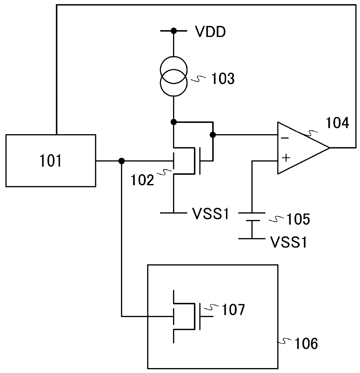
[0035]FIG. 1 is a block diagram of a semiconductor device of one embodiment of the present invention. The semiconductor device of one embodiment of the present invention includes a variable bias circuit 101, a transistor 102 for monitoring a threshold voltage, a current source 103, a differential amplifier 104, a reference voltage source 105, a functional circuit 106 using an oxide semiconductor, and an oxide semiconductor transistor 107. Here, the functional circuit 106 is a circuit which includes the oxide semiconductor transistor 107 having a controlled back gate, and is generally a memory, an arithmetic circuit, an amplifier circuit, or the like; however, one embodiment of the present invention is not limited thereto.

[0036]Components will be described below. The variable bias circuit 101 is a voltage-controlled voltage source which is controlled by an input voltage and generates voltage to be applied to a back gate (back gate control voltage Vbg). The transistor 102 for monitori...

embodiment 2

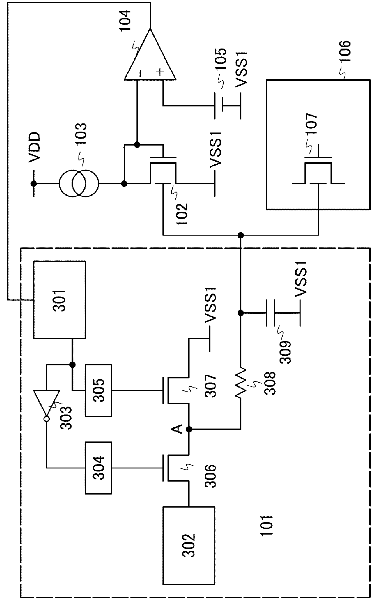
[0040]FIG. 3 is a more specific block diagram of the variable bias circuit 101. The variable bias circuit illustrated in FIG. 3 includes a PWM wave generation circuit 301, a constant voltage circuit 302, an inverter 303, level shifters 304 and 305, switch transistors 306 and 307, a resistor 308, and a capacitor 309. The PWM wave generation circuit 301 is a signal generation circuit capable of controlling a duty ratio in accordance with an input voltage.

[0041]The PWM wave generation circuit 301 is controlled by the output voltage of the differential amplifier 104; when the output voltage of the differential amplifier 104 is increased, a period during which the output of the PWM wave generation circuit 301 is at a high level is short, and when the output voltage of the differential amplifier 104 is decreased, a period during which the output of the PWM wave generation circuit 301 is at a low level is short. The output of the PWM wave generation circuit 301 is connected to a gate of th...

embodiment 3

[0047]FIG. 6 shows an example in which an oxide semiconductor transistor is used for a memory circuit. The memory cell 200 includes a write transistor 201, a read transistor 202, and a storage capacitor 203. The case where the write transistor 201 is an oxide semiconductor transistor and the read transistor 202 is a p-channel Si transistor is described. The read transistor 202 may be an n-channel Si transistor or an oxide semiconductor transistor. Note that the memory circuit in this embodiment corresponds to the functional circuit 106 in the above embodiment, and the write transistor 201 corresponds to the oxide semiconductor transistor 107 described in the above embodiment.

[0048]A gate of the write transistor 201 is connected to a word line 204, and one of a source and a drain of the write transistor 201 is connected to a gate of the read transistor 202 and one electrode of the storage capacitor 203. The other electrode of the storage capacitor 203 is connected to a capacitor word...


PUM


Abstract

To stably control a threshold voltage of a functional circuit using an oxide semiconductor. A variable bias circuit, a monitoring oxide semiconductor transistor including a back gate, a current source, a differential amplifier, a reference voltage source, and a functional circuit which includes an oxide semiconductor transistor including a back gate are provided. The current source supplies current between a source and a drain of the monitoring oxide semiconductor transistor to generate a gate-source voltage in accordance with the current. The differential amplifier compares the voltage with a voltage of the reference voltage source, amplifies a difference, and outputs a resulting voltage to the variable bias circuit. The variable bias circuit is controlled by an output of the differential amplifier and supplies voltage to the back gate of the monitoring oxide semiconductor transistor and the back gate of the oxide semiconductor transistor included in the functional circuit.

Description

TECHNICAL FIELD[0001]The present invention relates to a semiconductor device which includes an oxide semiconductor transistor including a back gate, particularly, a semiconductor device having a function of automatically controlling voltage applied to a back gate. The present invention relates to an electronic device including the semiconductor device.BACKGROUND ART[0002]Memories such as an SRAM and a DRAM have already been used in a variety of electronic devices. For example, an SRAM or a DRAM is widely used as a cache memory. A cache memory is used in a central processing unit (CPU), a hard disk drive (HDD), a solid state drive (SSD), or the like. A cache memory is provided to input or output data to a logic circuit quickly.[0003]Although an example of nonvolatile memories includes a flash memory, response speed of a flash memory is low. As a novel memory, a memory using an oxide semiconductor has been proposed.[0004]The off-state current of a transistor using an oxide semiconduct...

Claims


Application Information

Patent Timeline
Patent Type & Authority Patents(United States)
IPC IPC(8): G11C5/14H01L29/786G11C11/24G11C19/28G11C16/34G11C7/12
CPCH01L29/7869G11C5/146G11C11/24G11C16/3418G11C19/28G11C7/12H01L27/1225G11C5/147
Inventor KOYAMA, JUN
Owner SEMICON ENERGY LAB CO LTD
Why Eureka
Try Eureka