

Post treatment methods for oxide layers on semiconductor devices
a post treatment method and semiconductor technology, applied in the direction of semiconductor devices, basic electric elements, electrical equipment, etc., can solve the problems of poor device performance or failure, high wafer or substrate temperature often required in thermal oxidation process, and the plasma process used to form oxide layers has problems to those presented by thermal oxidation processing, so as to improve the interface between silicon and silicon dioxide, improve oxygen content, and reduce the effect of oxide layer thickness changes
- Summary
- Abstract
- Description
- Claims
- Application Information
AI Technical Summary
Benefits of technology
Problems solved by technology
Method used
Image

Examples
examples
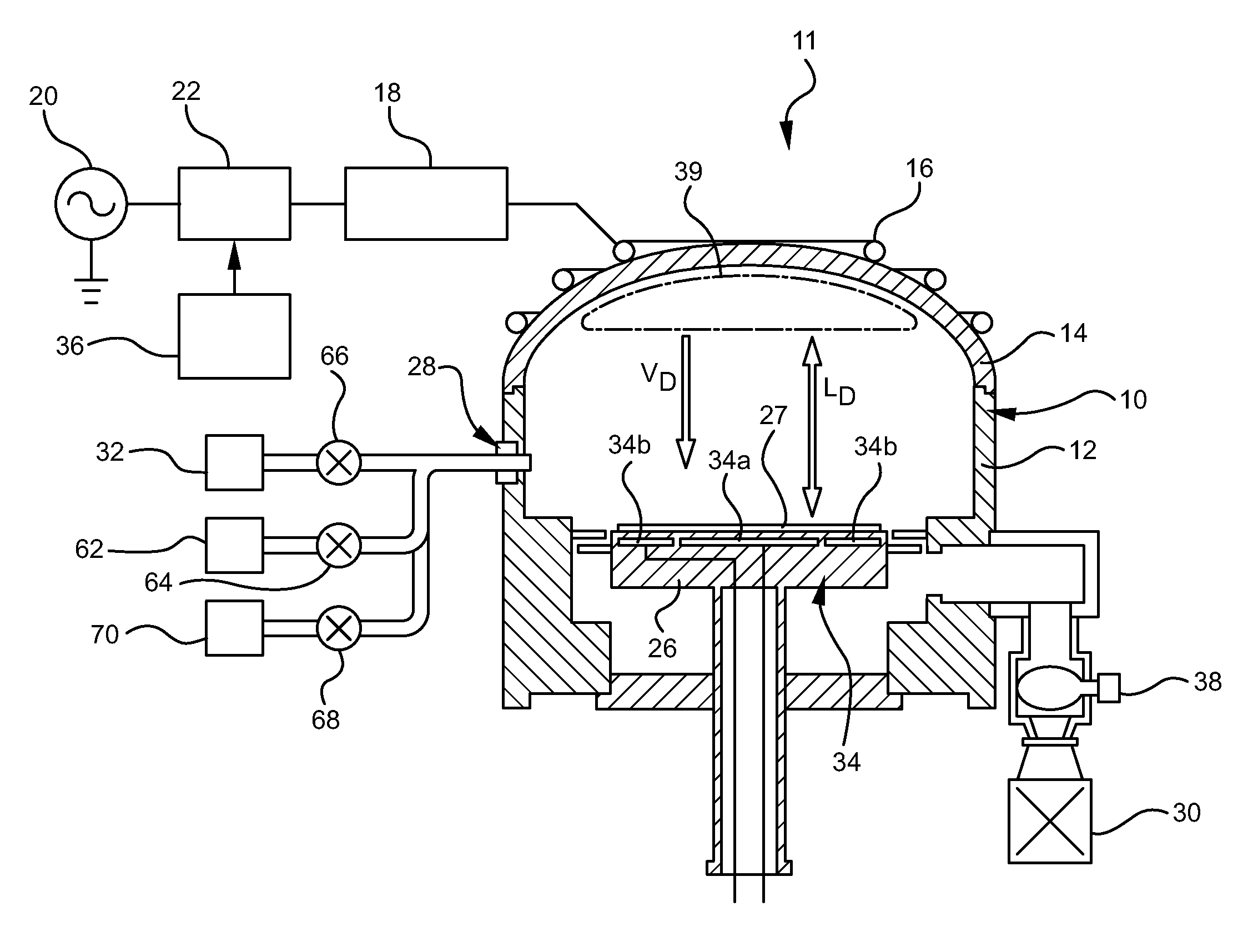
[0050]SiO2 layers were formed on four silicon substrates (Substrates A-D). The SiO2 layers were formed in a decoupled plasma oxidation (“DPO”) reactor using plasma oxidation. The initial thickness of the SiO2 layer on Substrates A-D, before post-treatment, measured 41 Angstroms
[0051]The SiO2 layer of substrate A was not subjected to post-treatment with a plasma in the DPO reactor but instead was annealed at a temperature of 1000° C. for 15 seconds in nitrogen gas in an RTA chamber. The SiO2 layer of substrate B was post treated with an argon plasma in the DPO reactor and annealed as described with reference to Substrate A. The SiO2 layer of Substrate C was post-treated with hydrogen plasma in the DPO reactor and annealed as described with reference to Substrate A. The SiO2layer of Substrate D was post treated with helium plasma in the DPO reactor and annealed as described with reference to Substrate A.
[0052]The “thickness shrinkage” of the SiO2 layers of Substrates A-D was measured ...
PUM
| Property | Measurement | Unit |
|---|---|---|
| temperature | aaaaa | aaaaa |
| temperature | aaaaa | aaaaa |
| temperature | aaaaa | aaaaa |
Abstract
Description
Claims
Application Information