

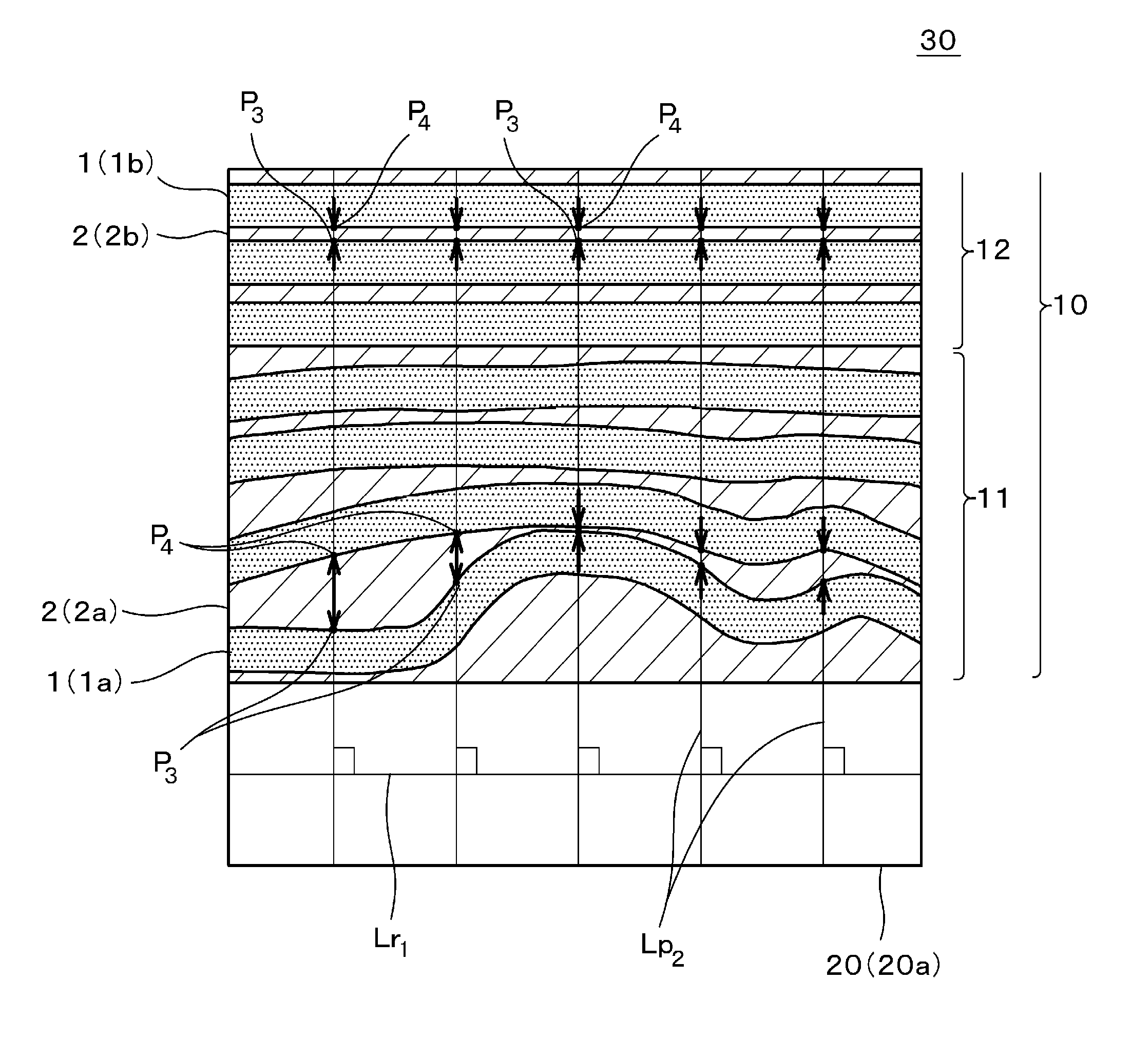
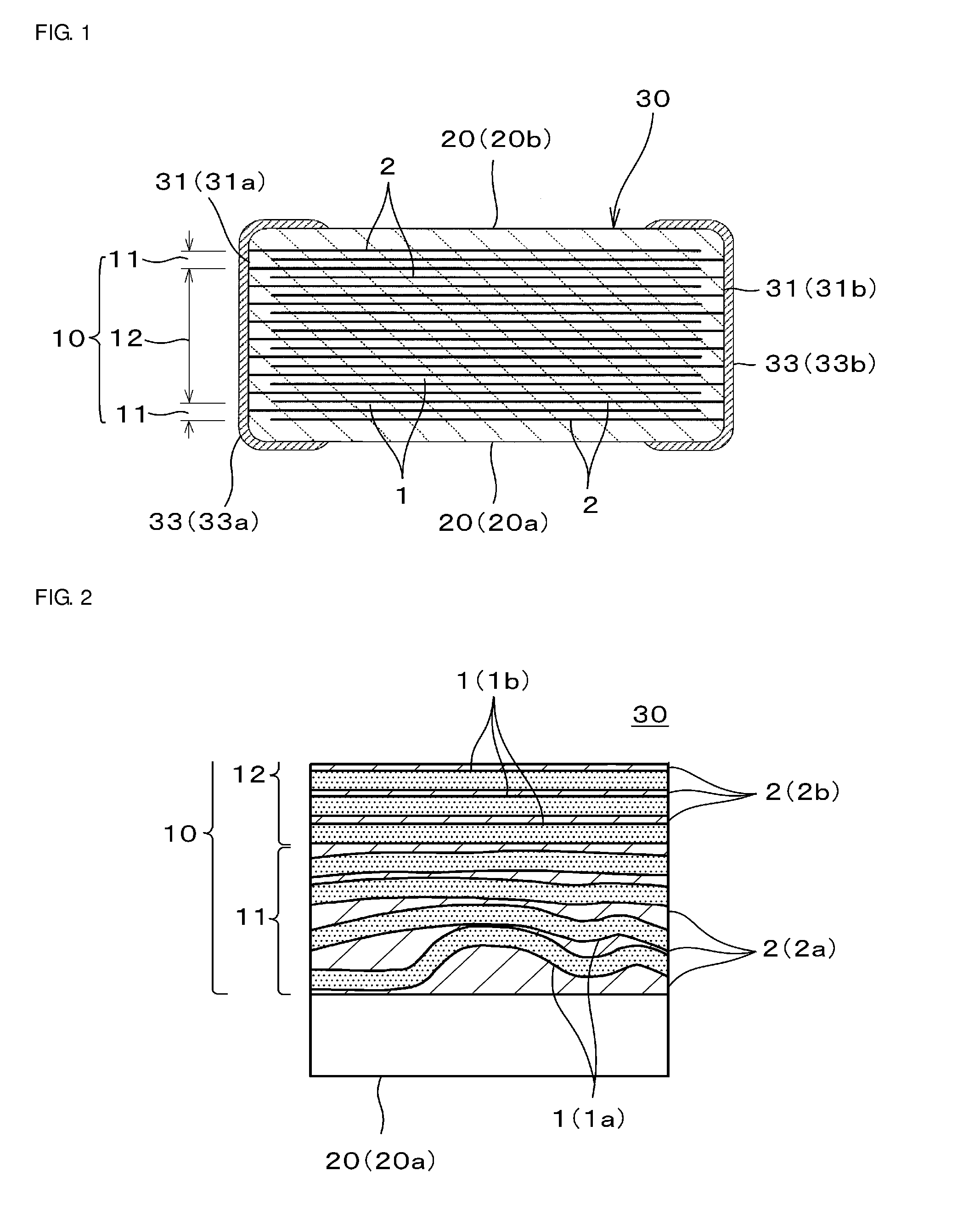
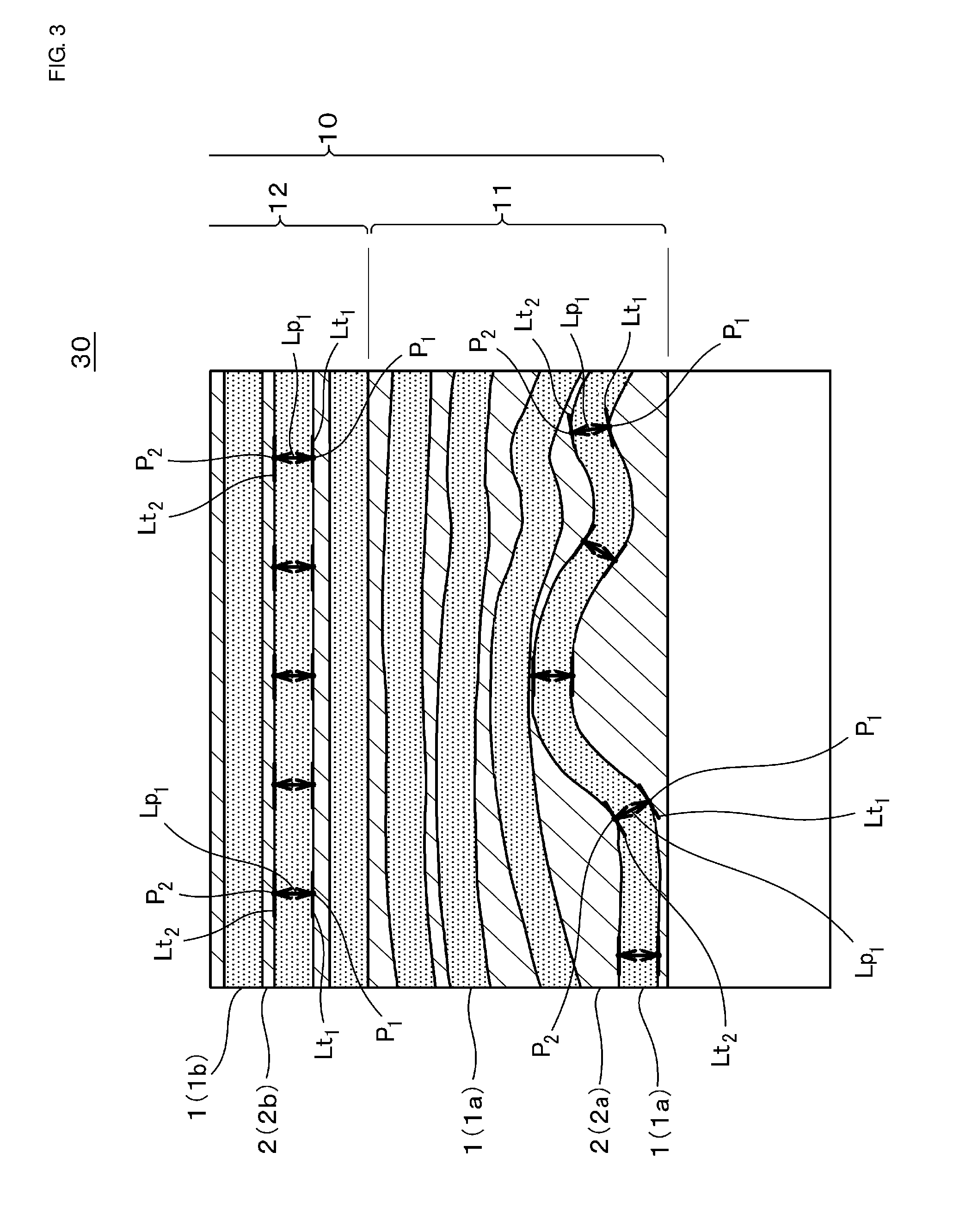
Multilayer ceramic electronic component
a technology of electronic components and ceramics, applied in the direction of fixed capacitor dielectrics, stacked capacitors, fixed capacitor details, etc., can solve the problems of internal stress caused by the difference in thermal expansion coefficient, cracks to occur in response, increased delamination, etc., to improve thermal shock resistance, high continuity, and small size
- Summary
- Abstract
- Description
- Claims
- Application Information
AI Technical Summary
Benefits of technology
Problems solved by technology
Method used
Image

Examples
example
[0097]In Example, chip-type multilayer ceramic capacitors were produced as multilayer ceramic electronic components, and the relationship between the sintering temperature rise rate in the sintering process, the structure of the multilayer portion, the occurrence rate of cracks in the thermal shock test, and the electrostatic capacity was examined.
[0098](A) Preparation of Ceramic Base Powder for Ceramic Layers (Dielectric Layers)
[0099]Base powder (ceramic base powder) for ceramic layers serving as dielectric layers was prepared in the following procedure.
[0100]First, BaCO3 powder and TiO2 powder were weighed such that the ratio of Ba to Ti (Ba / Ti) was 1.001. These powders were wet-ground and mixed in a zirconia ball mill.
[0101]After being dried, the powder mixture was heated to 900° C. or more and subjected to heat treatment (calcination), which produced a perovskite-type compound oxide (BaTiO3 ceramic powder) having an average particle diameter of 0.20 μm.
[0102]Then 0.6 mol parts o...
PUM
| Property | Measurement | Unit |
|---|---|---|
| particle diameter | aaaaa | aaaaa |
| particle diameter | aaaaa | aaaaa |
| width | aaaaa | aaaaa |
Abstract
Description
Claims
Application Information