Mass production process of high voltage and high current Schottky diode with diffused design

Active Publication Date: 2016-11-22
CHONGQING PINGWEI ENTERPRISE
View PDF11 Cites 3 Cited by
  • Summary
  • Abstract
  • Description
  • Claims
  • Application Information

AI Technical Summary

Benefits of technology

[0037]The advantageous effect of the process of the present invention includes the followings: The process of manufacturing JBS Schottky diode in diffused design of the present invention is particular suitable for high current chip technology, where the cost is at least lowered by one third when compared to epitaxial process. Also,

Problems solved by technology

However, the existing epitaxial process has the d

Method used


Image

  • Mass production process of high voltage and high current Schottky diode with diffused design
  • Mass production process of high voltage and high current Schottky diode with diffused design
  • Mass production process of high voltage and high current Schottky diode with diffused design

Examples


Example

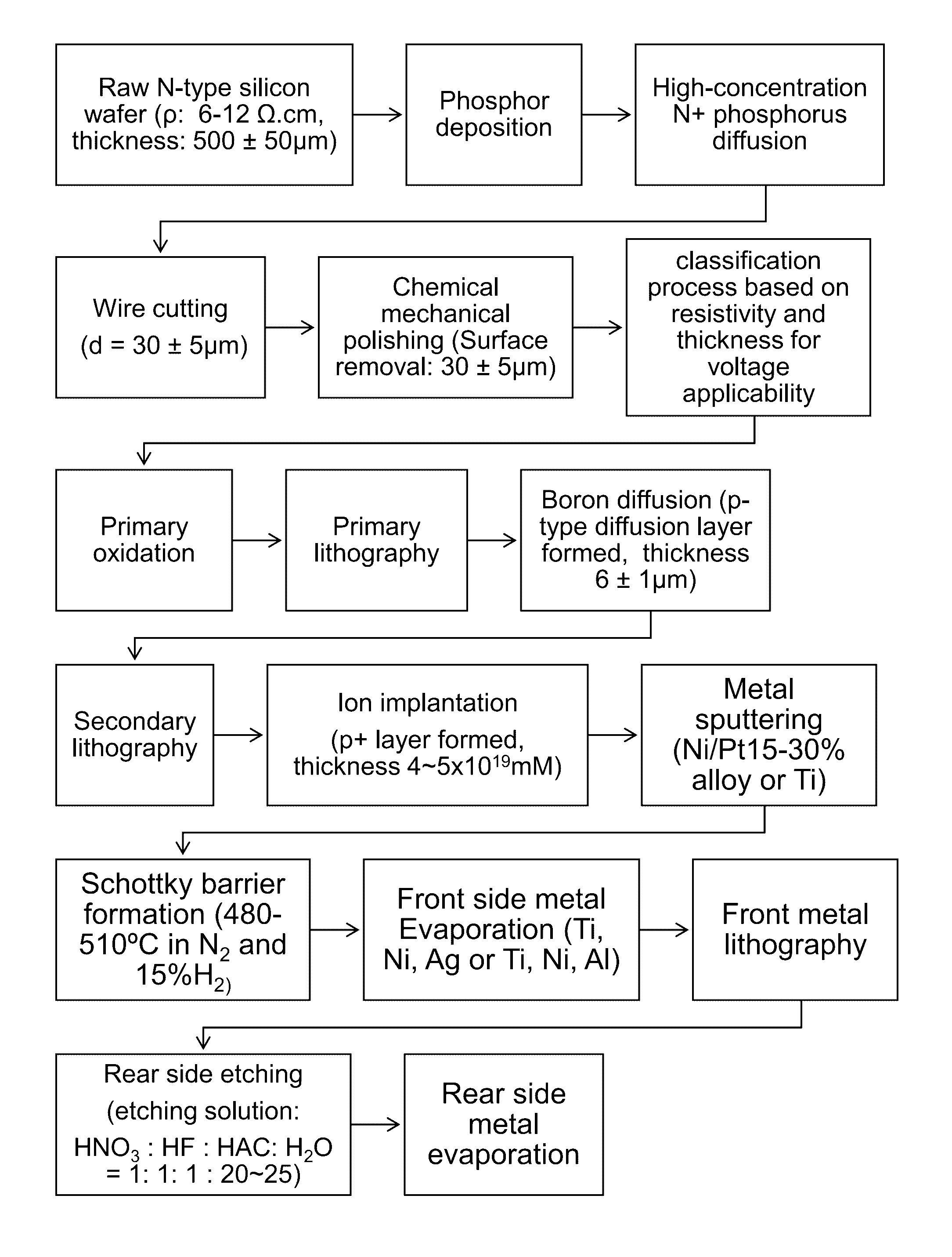
[0059]The present invention is further described in details with the accompanying drawings and embodiments.

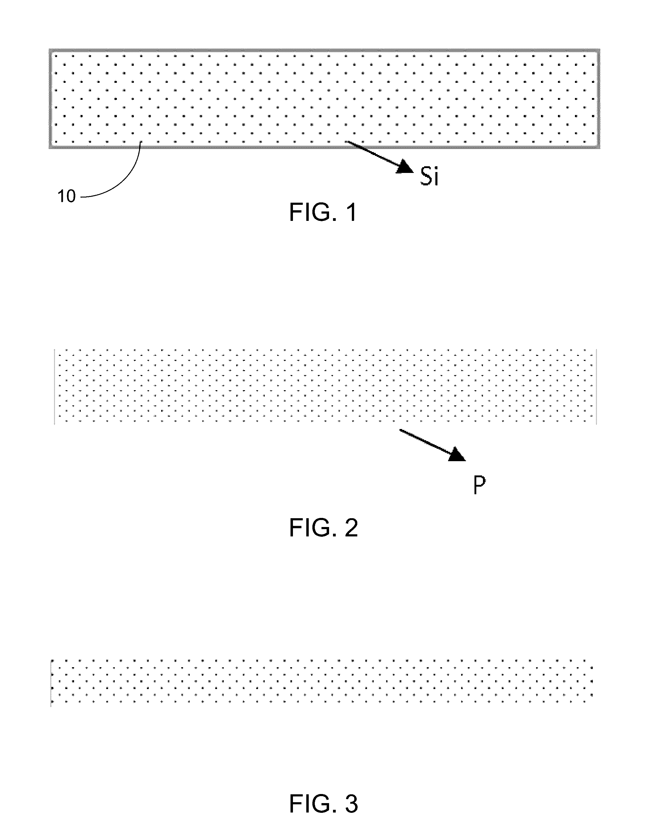
[0060]FIGS. 1-15 refers to an illustration of the step by step manufacturing process according to the process of manufacturing high voltage and high current Schottky diode with diffused design according to the preferred embodiment of the present invention. FIG. 16 is a flow chart showing the process of manufacturing high voltage and high current Schottky diode with diffused design according to the preferred embodiment of the present invention.

[0061]Referring to FIGS. 1-16 of the drawings, a process of manufacturing JBS Schottky diode according to a preferred embodiment of the present invention comprises the following steps:

[0062](a) Select a raw N-type silicon wafer 10. Preferably, as shown in FIG. 1, the raw silicon wafer 10 has a resistivity ρ=6-12 Ω·cm; and a thickness t of 500±50 μm.

[0063](b) Process high-concentration phosphor deposition for the raw silicon wafer 10. FIG. ...


PUM


Abstract

A process of manufacture of high voltage (300-600V) and high current (10-100 A) Schottky diode, which includes the following steps in sequence: provide a N-type silicon wafer; process phosphor deposition and high-concentration N+ phosphorus diffusion; cutting and chemical mechanical polishing; classifying into different voltage groups; processing primary oxidation and lithography; processing boron diffusion, secondary lithography and wiring; process ion implantation and metal spluttering to form the Schottky barrier; process metal evaporation and lithography for front metal; and finally process etching and metal evaporation for rear metal. Instead of the conventional epitaxial process, a diffusion process is employed to form the N+ layer. The final product is equipped with the advantages of Schottky diode and is applicable for high voltage of 300-600V and high current of 10-100 A. The current leakage and defect rate are dramatically lowered while the cost is lowered, thus mass production is facilitated.

Description

BACKGROUND OF THE PRESENT INVENTION[0001]1. Field of Invention[0002]The present invention relates to a production process of silicon chips, and more particularly to a JBS (Junction Barrier Schottky) diode production process, which belongs to the field of manufacture of high voltage (300-600V) and high current (10-100 A) Schottky diode.[0003]2. Description of Related Arts[0004]Schottky components belongs to surface semiconductor components and its maximum voltage is 200V. When Schottky barrier components are integrated with traditional p / n junction diodes, its reverse breakdown voltage (vbr) can be increased to above 300V. Since the advantages of Schottky barrier in forward conduction can be utilized, the forward voltage drop of 0.75V is made possible. For silicon semiconductor, which is suitable for manufacture of 300-600V high current (10-100 A) components, Schottky components have unique technical advantages to replace the existing Fast Recovery Diode (FRD). All of the existing li...

Claims


Application Information

Patent Timeline
IPC IPC(8): H01L29/872H01L21/304H01L29/47H01L21/225H01L21/306H01L21/265H01L21/285H01L21/66H01L29/861H01L29/66H01L21/302H01L21/78
CPCH01L29/66143H01L21/2251H01L21/78H01L21/30625H01L21/26513H01L21/2855H01L21/30604H01L22/20H01L22/12H01L22/14H01L29/861H01L29/47H01L29/872H01L21/304H01L21/302H01L29/8611H01L21/28537H01L29/0619H01L29/401
Inventor WANG, XINGLONGLI, SHUZHOUZHANG, LIXU, XIANGTAO
Owner CHONGQING PINGWEI ENTERPRISE
Why Eureka
Try Eureka