Appendage mountable electronic devices conformable to surfaces

a technology of electronic devices and surfaces, applied in external electrodes, surgical manipulators, surgical robots, etc., can solve the problems of difficult to reliably provide electronics on a correspondingly complex surface, poor application suited to clinical applications outside of research labs or clinical settings, etc., to reduce the volume of the enclosure, reduce the diameter of the enclosure, and reduce the fracture strain of the elastomeric substra

Active Publication Date: 2017-01-24
THE BOARD OF TRUSTEES OF THE UNIV OF ILLINOIS
View PDF506 Cites 79 Cited by
  • Summary
  • Abstract
  • Description
  • Claims
  • Application Information

AI Technical Summary

Benefits of technology

[0039]Any of the systems provided herein may have at least a portion of the flexible or stretchable electronic device supported by either the outer surface, by the inner surface of the flexible or stretchable substrate, or by both surfaces. In an aspect, the inner surface and outer surface are interchangeably flippable without substantial degradation of a functionality parameter of the one or more sensors, actuators or both supported by the inner surface or the outer surface of the flexible or stretchable substrate.
[0124]Also provided herein are related methods for making or for using any of the devices disclosed herein. Various physical characteristics of the devices provide the ability to specially manipulate the device to achieve functional benefit. For example, the substrate is capable of being shaped to any desired surface and an electronically active material transferred thereto. For transfer printing, the outer surface of the substrate is configured as a receiving surface of the electronically active material as the outer-facing surface is generally more accessible than an inner-facing surface. The deformability of the substrate provides the ability to then flip the receiving surface from an outer-facing configuration to an inner-facing configuration, thereby facilitating intimate contact between the electronically active material with a biological surface when the device is mounted or applied to the biological surface.

Problems solved by technology

These systems have many important capabilities, but they are poorly suited for practical application outside of research labs or clinical settings, due to difficulties in establishing long-lived, robust electrical contacts that do not irritate the skin, and in achieving integrated systems with overall sizes, weights and shapes that do not cause discomfort during prolonged use.
One difficulty with providing electronics to interact with such complex surface shapes is that it can be difficulty to reliably provide electronics in a correspondingly complex surface shape so as to achieve good interaction between the electronics and the complex surface shape over a large contact area.

Method used


Image

  • Appendage mountable electronic devices conformable to surfaces
  • Appendage mountable electronic devices conformable to surfaces
  • Appendage mountable electronic devices conformable to surfaces

Examples


example 1

Silicon Nanomembranes for Fingertip Electronics

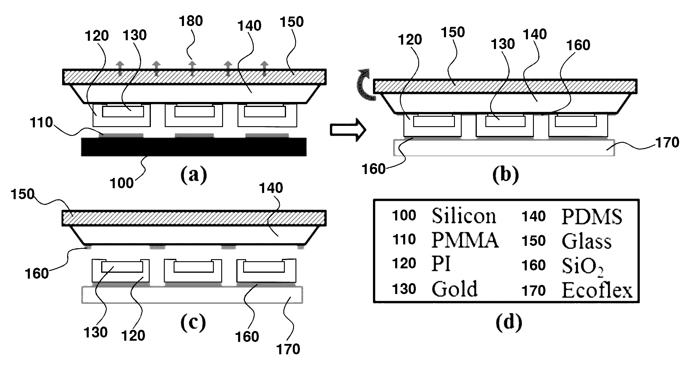
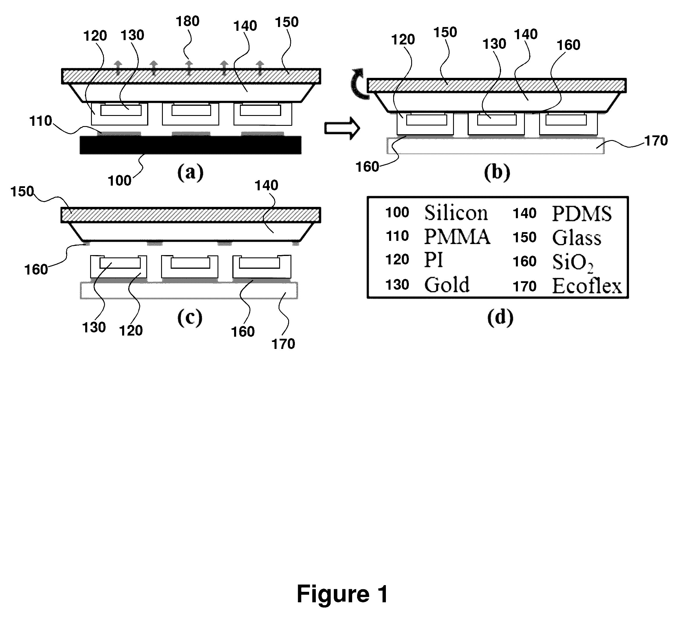
[0201]This example relates to the use of semiconductor nanomaterials, advanced fabrication methods and unusual device designs for a class of electronics capable of integration onto the inner and the outer surfaces of thin, elastomeric sheets in closed-tube geometries, specially formed for mounting on the fingertips. Multifunctional systems of this type allow electrotactile stimulation with electrode arrays multiplexed using silicon nanomembrane (Si NM) diodes, high-sensitivity strain monitoring with Si NM gauges, and tactile sensing with elastomeric capacitors. Analytical calculations and finite element modeling of the mechanics quantitatively capture the key behaviors during fabrication / assembly, mounting and use. The results provide design guidelines that highlight the importance of the NM geometry in achieving the required mechanical properties. This type of technology is compatible with applications ranging from human-machine interf...

example 2

Methods of Making the Electronic Devices

[0216]1. Electrotactile Arrays:

[0217]a. Cut 1′×1′ SOI wafers ((110), 300 nm Si) and clean with acetone and IPA.

[0218]b. Form a 900 nm layer of SiO2 by PECVD as p-dope diffusion mask.

[0219]c. Pattern diffusion mask by: i. Pattern photoresist (PR) AZ5214: Spin coat PR AZ5214 (3000 rpm, 30 s), pre-bake (110° C., 1 min), align mask and expose, develop with MIF327 (40 s), post-bake (110° C., 3 min). ii. Wet etch with buffered oxide etchant (BOE) (NH4F: HF=6:1) for 1.5 min and remove PR with acetone.

[0220]d. P-type doping: i. Clean wafers with Nano-strip™ (Cyantek), place next to boron doping source, and put into furnace (1000° C.) for 30 min. ii. Etch SiO2 mask completely with HF (30 sec), and form another 900 nm layer of SiO2 by PECVD as n-dope diffusion mask. iii. Pattern diffusion mask: Same as 1c.

[0221]e. N-type doping: i. Clean wafers with Nano-Strip™, place next to phosphorous doping source at 1000° C. for 10 min. ii. Etch SiO2 mask completel...

example 3

Appendage Mountable Electronic Devices Conformable to Biological Surfaces

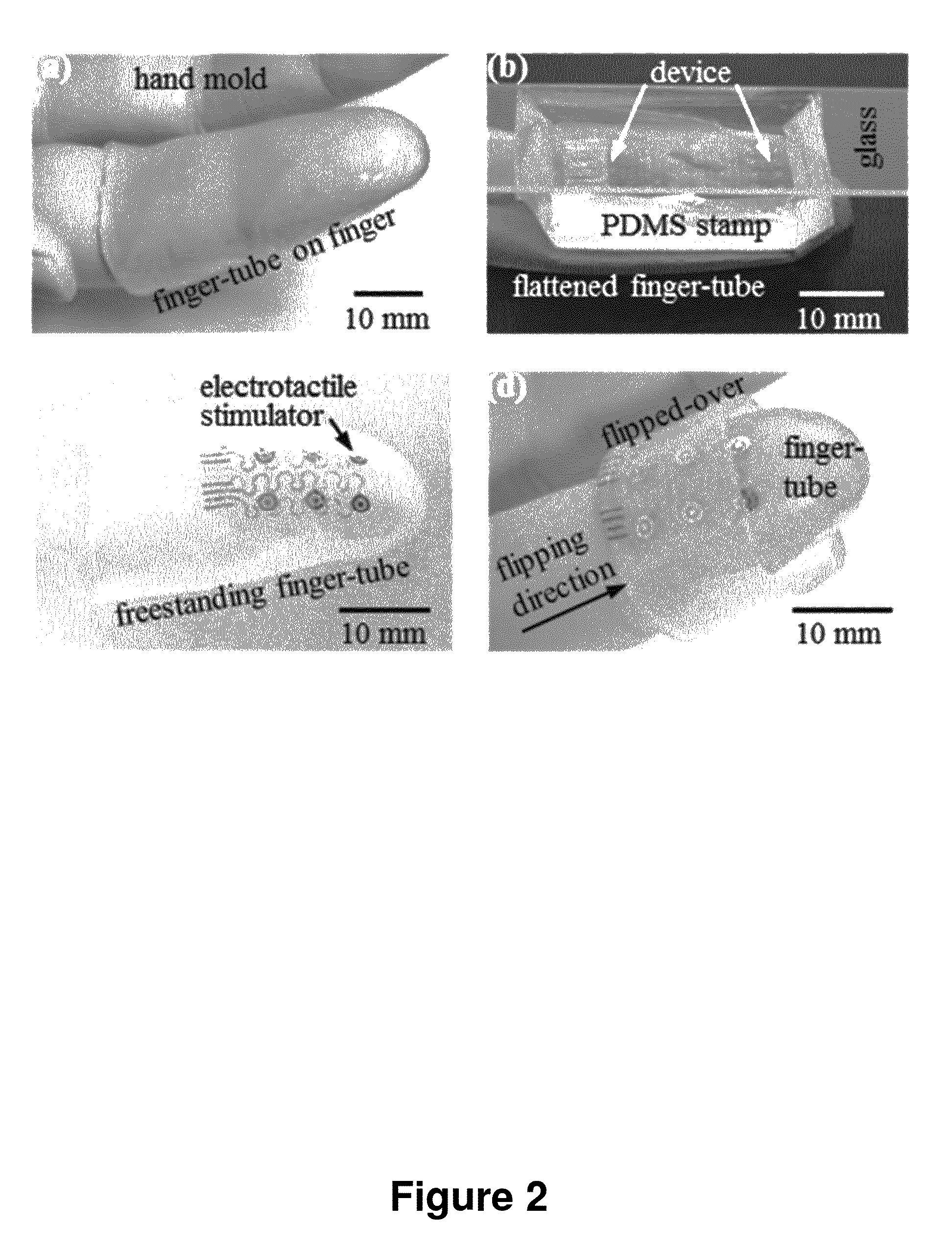
[0284]One example of an appendage mountable electronic system is schematically summarized in FIGS. 14-17, including an appendage corresponding to a finger or a finger-tip. Different views of an appendage mountable electronic system 10 is provided in FIG. 14(A-C), with a top view (A), a side cross-section view (B) and a cross-section viewed from an end (C). Referring to the different views of FIG. 14, the system 10 comprises a flexible and stretchable substrate 20 having an inner surface 30 and an outer surface 40. In this example, the electronic device 50 comprises a plurality of flexible or stretchable sensors 54 supported by the outer surface 40, and a plurality of flexible or stretchable actuators 55 supported by the inner surface 30. The electronic device further comprises various components to provide desired functionality and operating characteristics. For example, FIG. 14 illustrates electrical interconn...


PUM

PropertyMeasurementUnit
thicknessaaaaaaaaaa
surface areaaaaaaaaaaa
diameteraaaaaaaaaa

Abstract

Disclosed are appendage mountable electronic systems and related methods for covering and conforming to an appendage surface. A flexible or stretchable substrate has an inner surface for receiving an appendage, including an appendage having a curved surface, and an opposed outer surface that is accessible to external surfaces. A stretchable or flexible electronic device is supported by the substrate inner and / or outer surface, depending on the application of interest. The electronic device in combination with the substrate provides a net bending stiffness to facilitate conformal contact between the inner surface and a surface of the appendage provided within the enclosure. In an aspect, the system is capable of surface flipping without adversely impacting electronic device functionality, such as electronic devices comprising arrays of sensors, actuators, or both sensors and actuators.

Description

CROSS-REFERENCE TO RELATED APPLICATIONS[0001]This application claims benefit to U.S. Provisional Patent Application Nos. 61 / 794,004 filed Mar. 15, 2013, 61 / 636,527 filed Apr. 20, 2012 and 61 / 618,371 filed Mar. 30, 2012, each of which are incorporated by reference to the extent not inconsistent herewith.STATEMENT REGARDING FEDERALLY SPONSORED RESEARCH OR DEVELOPMENT[0002]This invention was made with government support under CMMI-0328162 and awarded by the National Science Foundation, and DE-FG02-07ER46471 and DE-FG02-07ER46453 awarded by the Department of Energy. The government has certain rights in the invention.BACKGROUND OF INVENTION[0003]Physiological measurement and stimulation techniques that exploit interfaces to the skin have been of interest for many years. Despite much progress over this time, nearly all associated device technologies continue to rely on conceptually old designs. Typically, small numbers of bulk electrodes are mounted on the skin via adhesive tapes, mechani...

Claims


Application Information

Patent Timeline
Patent Type & Authority Patents(United States)
IPC IPC(8): H05K1/00H05K7/02A61B5/00A41D19/015A61B5/11H05K3/00H01L23/538A61B5/01H05K1/02
CPCH05K7/02A41D19/015A61B5/1125A61B5/483A61B5/6806A61B5/6826A61B5/6843A61B5/7455A61B34/35A61B34/76H01L23/5388H05K3/0014A61B5/01A61B5/4875A61B2034/741A61B2505/05A61B2562/028A61B2562/0209A61B2562/029A61B2562/0233A61B2562/0247A61B2562/0261A61B2562/0271A61B2562/0285A61B2562/046A61B2562/12A61B2562/164A61B2562/227H01L2224/95H01L2924/0002H05K1/0283Y10T29/49124H01L2924/00H01L2224/95001A61B5/053A61N1/04A61N1/36A61N1/3603A61B5/24Y10S439/909A61N1/0456A61N1/0476A61B42/10H05K1/11H05K1/162H05K1/189H05K3/303H05K2201/0133H05K2201/055H05K2201/10098H05K2201/10151
Inventor ROGERS, JOHN AYING, MINGBONIFAS, ANDREWLU, NANSHU
Owner THE BOARD OF TRUSTEES OF THE UNIV OF ILLINOIS
Why Eureka
Try Eureka