Silicon carbide epitaxial wafer, method for manufacturing silicon carbide epitaxial wafer, device for manufacturing silicon carbide epitaxial wafer, and silicon carbide semiconductor element

a technology of silicon carbide and epitaxial wafer, which is applied in the direction of crystal growth process, polycrystalline material growth, chemically reactive gas growth process, etc., can solve the problem that further performance improvement cannot be anticipated for silicon semiconductor devices, and achieve the effect of reducing the surface defect density and high reliability

Inactive Publication Date: 2017-03-07
NAT INST OF ADVANCED IND SCI & TECH
View PDF13 Cites 0 Cited by
  • Summary
  • Abstract
  • Description
  • Claims
  • Application Information

AI Technical Summary

Benefits of technology

[0023]According to the present invention, the various problems in related art can be solved, and it is possible to provide a silicon carbide epitaxial wafer in which the occurrence of giant step bunchings (GSBs) caused by basal plane dislocations (BPDs) that occur during hydrogen etching is suppressed on a low off-angle silicon carbide substrate to decrease the surface defect density of an epitaxially grown layer to allow the formation of a silicon carbide semiconductor device having high reliability, a method for manufacturing the wafer, and an apparatus for manufacturing the wafer, and a silicon carbide semiconductor device having the wafer.

Problems solved by technology

So far, the performance of power semiconductor devices has been improved using silicon (Si) semiconductors, but a situation has been reached in which further performance improvement cannot be anticipated for silicon semiconductor devices because of the Si physical property limit.

Method used


Image

  • Silicon carbide epitaxial wafer, method for manufacturing silicon carbide epitaxial wafer, device for manufacturing silicon carbide epitaxial wafer, and silicon carbide semiconductor element
  • Silicon carbide epitaxial wafer, method for manufacturing silicon carbide epitaxial wafer, device for manufacturing silicon carbide epitaxial wafer, and silicon carbide semiconductor element
  • Silicon carbide epitaxial wafer, method for manufacturing silicon carbide epitaxial wafer, device for manufacturing silicon carbide epitaxial wafer, and silicon carbide semiconductor element

Examples


example 1

[0075]A typical silicon carbide substrate having a 4H crystal structure was provided as a silicon carbide substrate having an α-type crystal structure. This silicon carbide substrate has a substrate surface in which the (0001) Si face is tilted in the direction at 0.9°.

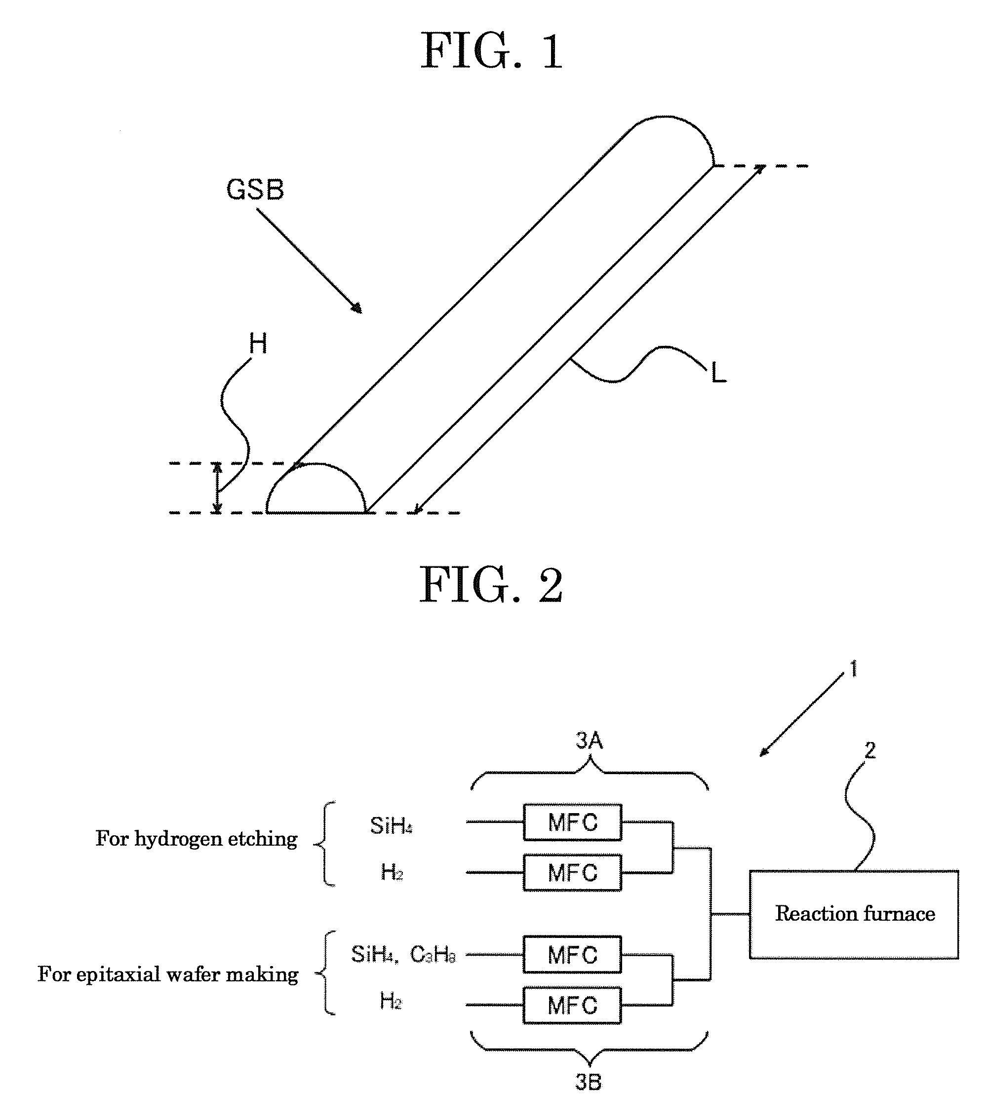
[0076]This silicon carbide substrate was placed in a reaction furnace 2 in a silicon carbide epitaxial wafer manufacturing apparatus 1 shown in FIG. 2, and a silicon carbide epitaxial wafer according to Example 1 was manufactured as follows. FIG. 2 is an explanatory diagram showing the schematic configuration of the silicon carbide epitaxial wafer manufacturing apparatus 1.

[0077]Here, the silicon carbide epitaxial manufacturing apparatus 1 has as a chemical vapor deposition apparatus a reaction furnace 2 having a gas discharge port allowing the adjustment of the pressure in the furnace via a discharge valve, a heating portion allowing the increase of the temperature in the furnace, an etching gas introduction port al...

example 3

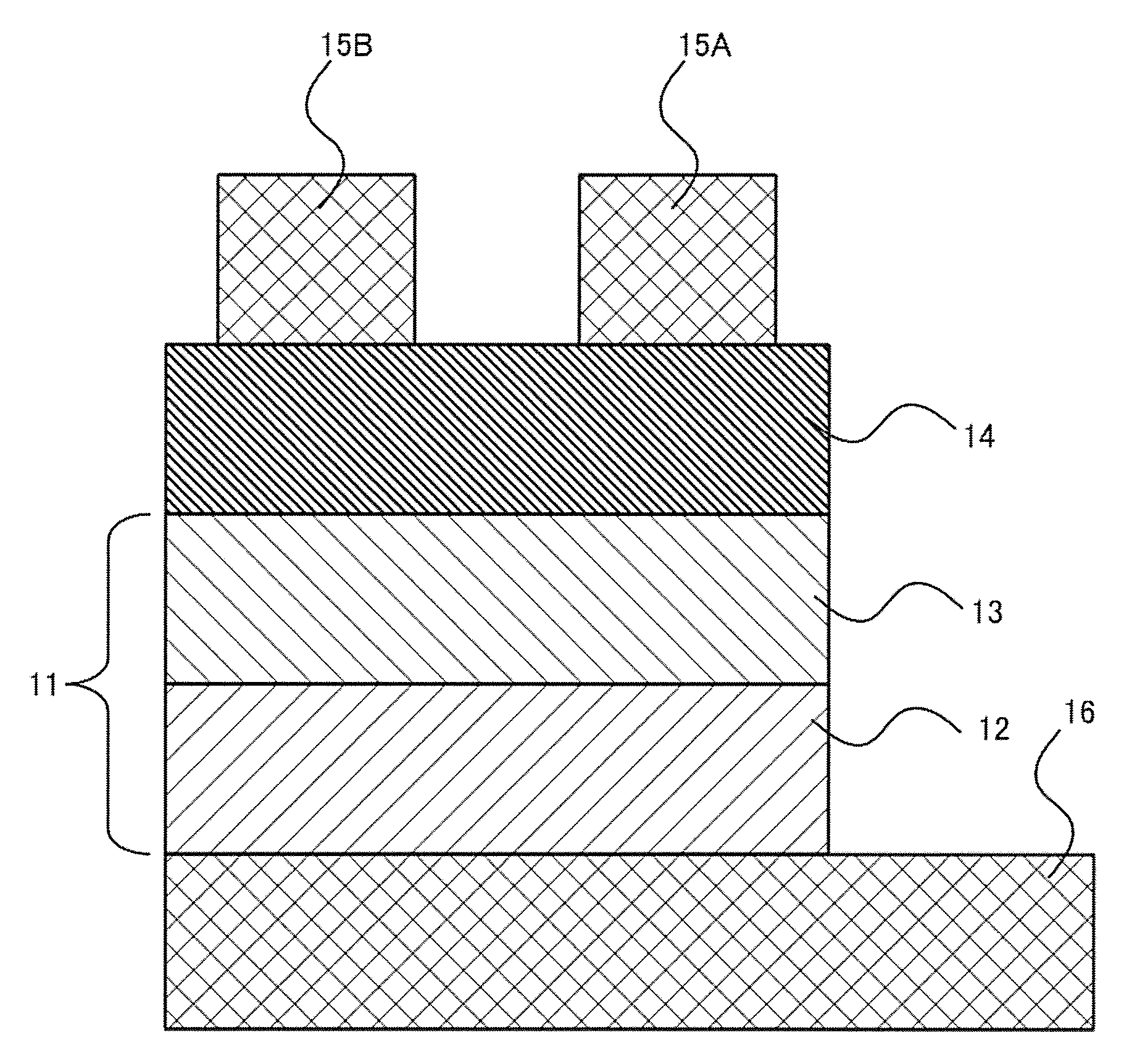
[0105]A silicon carbide semiconductor device according to Example 3 having the device structure of a MOS capacitor shown in FIG. 9 was manufactured. FIG. 9 is a cross-sectional view showing the schematic configuration of the device structure of a MOS capacitor. Here, numeral 11 denotes a silicon carbide epitaxial wafer, numeral 12 denotes a silicon carbide substrate, numeral 13 denotes an epitaxially grown layer, numeral 14 denotes a silicon dioxide layer, numerals 15A and 15B denote upper electrodes, and numeral 16 denotes a lower electrode.

[0106]First, a silicon carbide epitaxial wafer in which the surface defect density of an epitaxially grown layer based on GSBs caused by BPDs was 16 / cm2 manufactured according to the manufacturing conditions in Example 1 was provided as the silicon carbide epitaxial wafer 11.

[0107]The surface of the epitaxially grown layer 13 of this silicon carbide epitaxial wafer 11 was oxidized in a 1,200° C.·O2 atmosphere by thermal oxidation to form the sil...


PUM

PropertyMeasurementUnit
depthaaaaaaaaaa
off-angleaaaaaaaaaa
off-angleaaaaaaaaaa

Abstract

To provide silicon carbide epitaxial wafer in which occurrence of giant step bunchings (GSBs) caused by basal plane dislocations (BPDs) that occur during hydrogen etching is suppressed on low off-angle silicon carbide substrate to decrease surface defect density of epitaxially grown layer to allow formation of silicon carbide semiconductor device having high reliability, method for manufacturing the wafer, and apparatus for manufacturing the wafer, and silicon carbide semiconductor device having the wafer.A silicon carbide epitaxial wafer of the present invention is such that epitaxially grown layer is disposed on silicon carbide substrate which has α-type crystal structure and in which (0001) Si face is tilted at greater than 0° and less than 5°, wherein surface defect density of the epitaxially grown layer based on giant step bunching caused by basal plane dislocation on substrate surface of the silicon carbide substrate is ≦20 / cm2.

Description

TECHNICAL FIELD[0001]The present invention relates to a silicon carbide epitaxial wafer having a few surface defects, a method for manufacturing the wafer, and an apparatus for manufacturing the wafer, and a silicon carbide semiconductor device having the wafer.BACKGROUND ART[0002]In power semiconductor devices, energy loss during power conversion is reduced, and energy saving can be expected. So far, the performance of power semiconductor devices has been improved using silicon (Si) semiconductors, but a situation has been reached in which further performance improvement cannot be anticipated for silicon semiconductor devices because of the Si physical property limit.[0003]On the other hand, silicon carbide (SiC) has excellent physical properties, a dielectric breakdown electric field strength about 10 times that of Si and a forbidden band width and a thermal conductivity about 3 times those of Si, and further performance improvement of power semiconductor devices can be expected, ...

Claims


Application Information

Patent Timeline
Patent Type & Authority Patents(United States)
IPC IPC(8): H01L29/15C30B25/20C30B25/18C30B29/36H01L29/16H01L29/04H01L21/3065H01L21/04H01L21/02
CPCC30B25/186C30B25/20C30B29/36H01L21/0262H01L21/02378H01L21/02433H01L21/02529H01L21/02658H01L21/0475H01L21/3065H01L29/04H01L29/045H01L29/1608H01L28/00
Inventor MASUMOTO, KEIKOKOJIMA, KAZUTOSHITAMURA, KENTARO
Owner NAT INST OF ADVANCED IND SCI & TECH
Why Eureka
Try Eureka