Display device including pixel electrode including oxide

a display device and pixel electrode technology, applied in the field of display devices, can solve the problems of increasing manufacturing costs, and achieve the effects of reducing manufacturing steps of display devices, low cost, and favorable characteristics

Active Publication Date: 2017-07-11
SEMICON ENERGY LAB CO LTD
View PDF182 Cites 2 Cited by
  • Summary
  • Abstract
  • Description
  • Claims
  • Application Information

AI Technical Summary

Benefits of technology

[0009]In the display device disclosed in Patent Document 3, a pixel electrode serving as one electrode of a capacitor needs to be formed in a step different from a step of forming an oxide semiconductor layer included in a transistor, which increases the manufacturing cost.
[0011]In view of the above problems, an object of one embodiment of the present invention is to provide a novel display device including a transistor that includes an oxide semiconductor and thus has favorable characteristics, a pixel electrode electrically connected to the transistor, and a capacitor electrically connected to the pixel electrode. Another object of one embodiment of the present invention is to provide a display device that can be manufactured at low cost.
[0014]Note that the second oxide semiconductor layer serving as the pixel electrode and the one electrode of the capacitor can also be referred to as an oxide semiconductor layer having high conductivity. The oxide semiconductor layer having high conductivity can be formed as follows. When hydrogen is added to an oxide semiconductor including oxygen vacancies, hydrogen enters oxygen vacant sites and forms a donor level in the vicinity of the conduction band. As a result, the conductivity of the oxide semiconductor layer is increased, so that the oxide semiconductor layer becomes conductive. Such an oxide semiconductor layer having become conductive can be referred to as an oxide conductor layer. An oxide semiconductor layer generally has a visible light transmitting property because of its large energy gap. An oxide conductor layer is an oxide semiconductor having a donor level in the vicinity of the conduction band. Therefore, the influence of absorption due to the donor level is small, and an oxide conductor layer has a visible light transmitting property comparable to that of an oxide semiconductor layer.
[0015]According to one embodiment of the present invention, the first oxide semiconductor layer serving as the channel formation region of the transistor and the second oxide semiconductor layer serving as the pixel electrode can be formed at the same time. Furthermore, the second oxide semiconductor layer also serves as the one electrode of the capacitor; thus, a step of further forming a conductive layer is unnecessary, reducing the manufacturing steps of the display device. This enables the display device to be manufactured at low cost.
[0018]According to one embodiment of the present invention, the one electrode of the capacitor is formed at the same time as the gate electrode of the transistor. The other electrode of the capacitor is formed at the same time as the oxide semiconductor layer of the transistor. Note that the other electrode of the capacitor also serves as the pixel electrode. In addition, the dielectric layer of the capacitor is formed at the same time as the gate insulating layer of the transistor. Thus, a step of further forming a conductive layer and / or a dielectric layer to form a capacitor and / or a pixel electrode is unnecessary, reducing the manufacturing steps of the display device. This enables the display device to be manufactured at low cost.
[0019]According to one embodiment of the present invention, it is possible to provide a novel display device including a transistor that includes an oxide semiconductor and thus has favorable characteristics and, a pixel electrode electrically connected to the transistor, and a capacitor electrically connected to the pixel electrode. Furthermore, the display device can be manufactured at low cost.

Problems solved by technology

In the display device disclosed in Patent Document 3, a pixel electrode serving as one electrode of a capacitor needs to be formed in a step different from a step of forming an oxide semiconductor layer included in a transistor, which increases the manufacturing cost.

Method used


Image

  • Display device including pixel electrode including oxide
  • Display device including pixel electrode including oxide
  • Display device including pixel electrode including oxide

Examples


embodiment 1

[0035]In this embodiment, a display device of one embodiment and a manufacturing method of the display device of one embodiment of the present invention will be described with reference to FIG. 1, FIG. 2, FIGS. 3A to 3C, FIGS. 4A to 4C, FIG. 5, FIGS. 6A to 6C, FIGS. 7A and 7B, and FIG. 8.

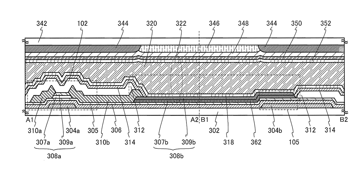
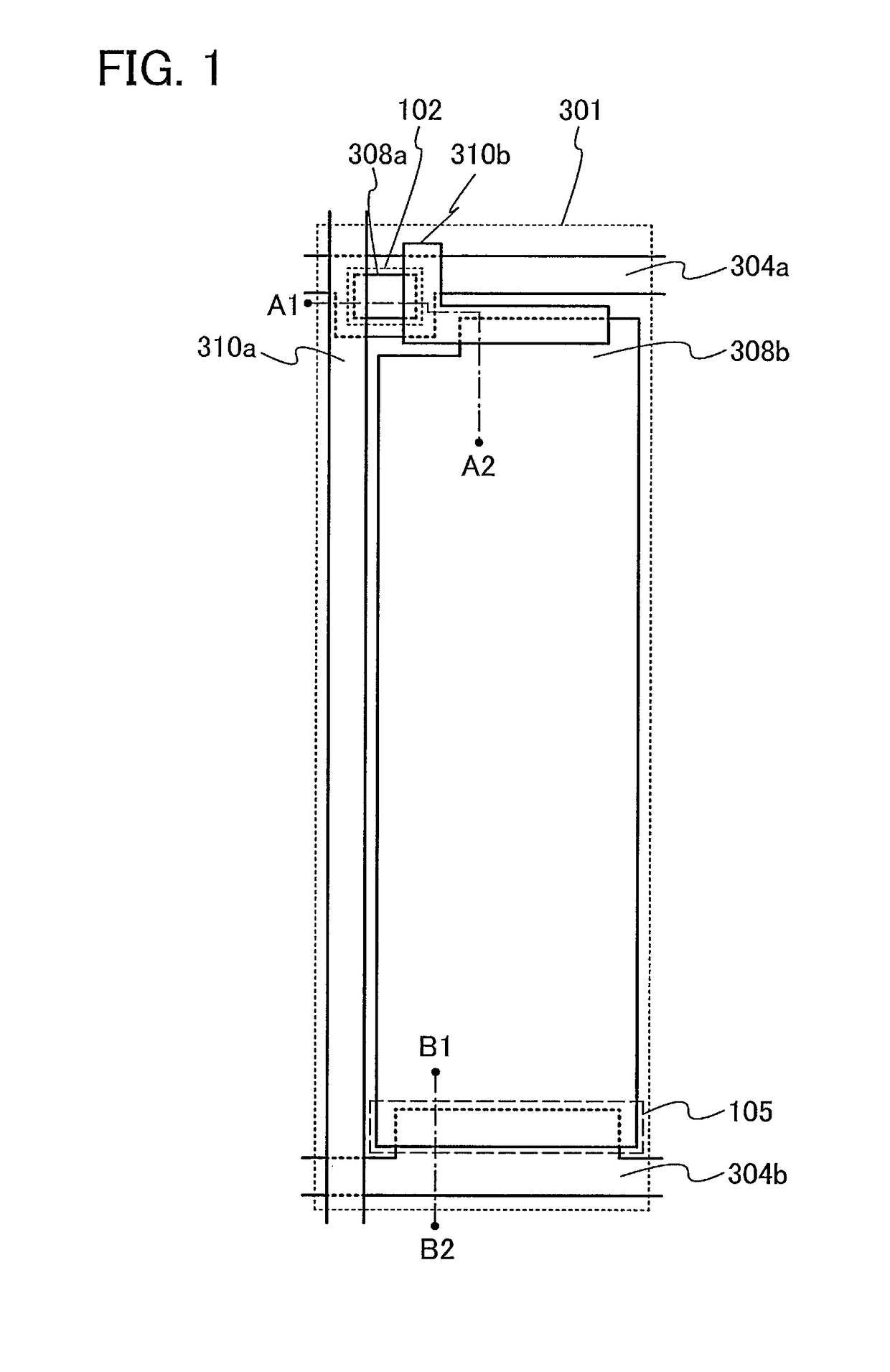
[0036]FIGS. 1 and 2 illustrate a structural example of the display device. FIG. 1 is a plan view of a pixel 301 included in a display device, and FIG. 2 is a cross-sectional view along dashed-dotted lines A1-A2 and B1-B2 in FIG. 1. Note that in FIG. 1, some components (e.g., insulating layers 305 and 306) of the pixel 301, a display element provided over the pixel 301, and the like are not illustrated for simplicity.

[0037]In the pixel 301 in FIG. 1, a conductive layer 304a serving as a scan line extends substantially perpendicularly to a signal line (in the horizontal direction in the drawing). The conductive layer 310a serving as the signal line extends substantially perpendicularly to the scan lin...

modification example 1

[0113]Next, modification examples of the transistor 102, the capacitor 105, and a pixel electrode that are included in a display device will be described with reference to FIG. 5. FIG. 5 is a cross-sectional view illustrating a modification example of the display device in FIG. 2. Portions similar to those in FIG. 2 and portions having functions similar to those of portions in FIG. 2 are denoted by the same reference numerals, and the detailed descriptions thereof are omitted.

[0114]The display device in FIG. 5 is different from the display device in FIG. 2 in that an opening 366 is formed instead of the opening 362.

[0115]The opening 366 can be formed by etching the insulating layers 312 and 314 so that the oxide semiconductor layer 308b is exposed, after the insulating layers 312 and 314 are successively formed. Specifically, an example of a method for manufacturing the display device illustrated in FIG. 5 will be described with reference to FIGS. 3A to 3C and FIGS. 6A to 6C.

modification example

Method for Manufacturing Display Device (Modification Example)

[0116]As in the manufacturing method described above, the conductive layers 310a and 310b and the insulating layer 312 are formed over the oxide semiconductor layers 308a and 308c (see FIG. 3C).

[0117]Then, the insulating layer 314 is formed over the insulating layer 312 (see FIG. 6A).

[0118]The insulating layers 312 and 314 are preferably formed successively in vacuum, in which case entry of impurities between the insulating layers 312 and 314 can be inhibited.

[0119]Next, the insulating layers 312 and 314 are processed into desired shapes, so that the opening 366 is formed (see FIG. 6B).

[0120]The opening 366 is formed so as to expose the oxide semiconductor layer 308c. An example of a formation method of the opening 366 includes, but not limited to, a dry etching method. Alternatively, a wet etching method or a combination of dry etching and wet etching can be employed for formation of the opening 366. The etching step for...


PUM

PropertyMeasurementUnit
drain voltageaaaaaaaaaa
off-state currentaaaaaaaaaa
channel lengthaaaaaaaaaa

Abstract

To provide a display device including a transistor that includes an oxide semiconductor and has favorable characteristics, a pixel electrode electrically connected to the transistor, and a capacitor electrically connected to the pixel electrode. To provide a display device that can be manufactured at low cost. The display device includes a display element including a pixel electrode, a transistor that performs switching of the display element and includes a first oxide semiconductor layer serving as a channel formation region, a capacitor that is electrically connected to the display element and includes a dielectric layer between a pair of electrodes. The pixel electrode is a second oxide semiconductor layer formed on the same surface as that on which the first oxide semiconductor layer is formed, and also serves as one electrode of the capacitor.

Description

BACKGROUND OF THE INVENTION[0001]1. Field of the Invention[0002]The present invention relates to a display device and an electronic device using the display device.[0003]2. Description of the Related Art[0004]Transistors used for most flat panel displays typified by a liquid crystal display device and a light-emitting display device are formed using silicon semiconductors such as amorphous silicon, single crystal silicon, and polycrystalline silicon provided over glass substrates. Further, transistors using such silicon semiconductors are used in integrated circuits (ICs) and the like.[0005]In recent years, attention has been drawn to a technique in which, instead of a silicon semiconductor, a metal oxide exhibiting semiconductor characteristics is used in transistors. Note that in this specification, a metal oxide exhibiting semiconductor characteristics is referred to as an oxide semiconductor.[0006]For example, such a technique is disclosed in which a transistor is fabricated usi...

Claims


Application Information

Patent Timeline
Patent Type & Authority Patents(United States)
IPC IPC(8): H01L27/12G02F1/1362
CPCH01L27/1255G02F1/136213H01L27/1225H01L27/1248H10K59/123H10K59/1213H10K59/1216G02F1/133345G02F1/13439G02F1/1368G02F2201/123G02F2202/10H01L29/7869
Inventor MIYAKE, HIROYUKIYAMAZAKI, SHUNPEI
Owner SEMICON ENERGY LAB CO LTD
Why Eureka
Try Eureka