Method for growing monocrystalline silicon and monocrystalline silicon ingot prepared thereof

Active Publication Date: 2017-12-05
ZING SEMICON CORP
View PDF5 Cites 0 Cited by
  • Summary
  • Abstract
  • Description
  • Claims
  • Application Information

AI Technical Summary

Benefits of technology

The present patent provides a method for growing monocrystalline silicon using the Czochralski method. This method involves melting silicon-containing materials in a crucible and pulling it to produce monocrystalline silicon. The method includes using silicon pieces with surface growth of silicon nitride and doping with deuterium, introducing a gas containing argon during the melting process, and applying a magnetic field during the pulling step. The resulting monocrystalline silicon can be used to produce wafers with a high nitrogen concentration.

Problems solved by technology

The oxygen precipitation defect may damage the integrated circuit device.
Recently, since thermal budget of integrated circuit manufacture process is significantly reduced, it cannot provide suitable conditions for oxygen precipitation within the silicon wafer and the intrinsic gettering effect is adversely affected.
The solid-phase nitrogen doping is able to control the nitrogen concentration, but it is difficult to obtain Si3N4 powder with high purity.
Si3N4 particle often remains because of its difficult melting property.
Therefore, dislocation free monocrystalline silicon cannot be formed.
The gas-phase nitrogen doping is achieved by the reaction of the nitrogen gas and the silicon melt, so that the purity is relatively high and the silicon nitride particle is not easily formed.
However, it is difficult to control the process and the nitrogen concentration since the reaction of gas-phase nitrogen doping is totally based on thermal convection.
Another problem, which has arisen in the semiconductor industry, is the degradation of device performance by hot carrier effects.

Method used


Image

  • Method for growing monocrystalline silicon and monocrystalline silicon ingot prepared thereof
  • Method for growing monocrystalline silicon and monocrystalline silicon ingot prepared thereof

Examples


examples

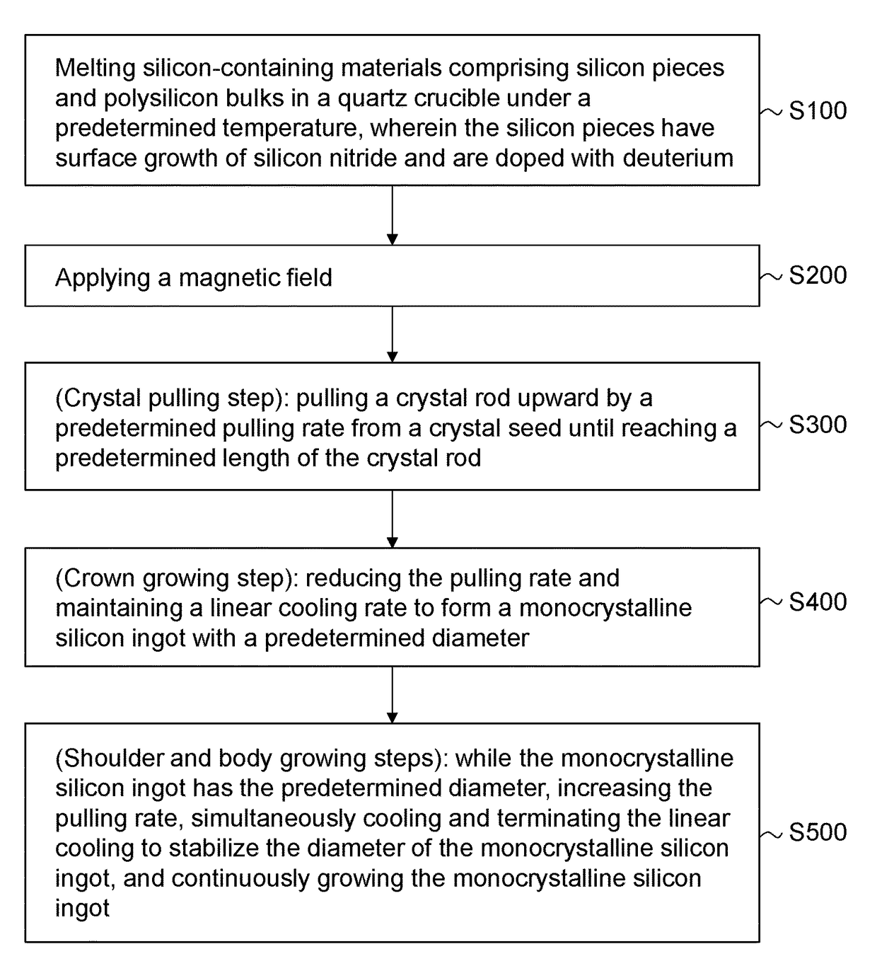
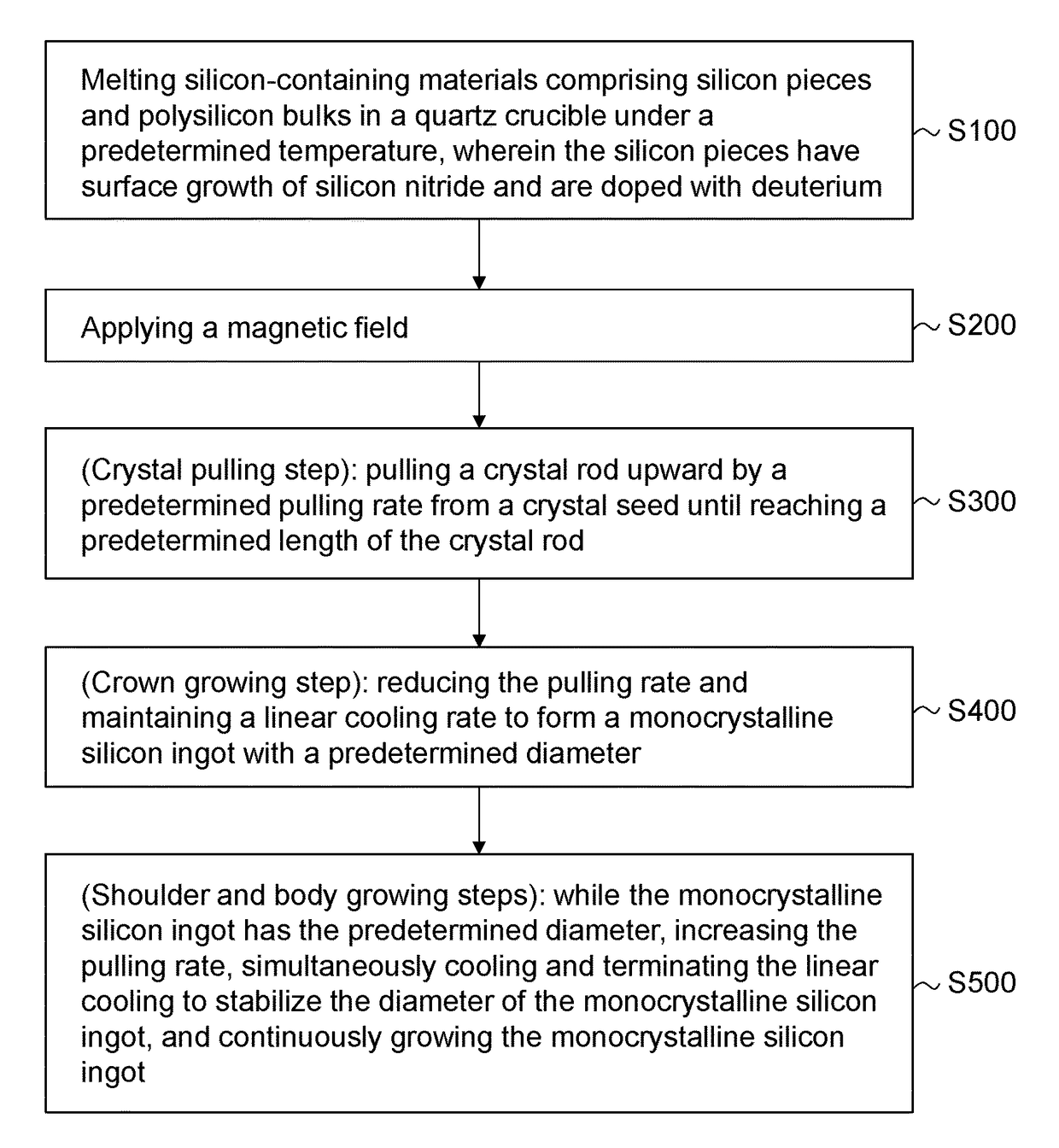
[0027]In the present application, solid-phase nitrogen doping as well as magnetic field Czochralski method (MCZ) is applied to the nitrogen doping of monocrystalline silicon. The process generally comprises the following steps: melting, seeding, crystal pulling, crown growing, shoulder growing, and body growing. FIG. 1 illustrates one embodiment of the method for growing monocrystalline silicon of the present application, which comprises:

[0028]S100: melting silicon-containing materials comprising silicon pieces and polysilicon bulks in a quartz crucible under a predetermined temperature, wherein the silicon pieces have surface growth of silicon nitride and are doped with deuterium;

[0029]S200: applying a magnetic field;

[0030]S300 (crystal pulling step): pulling a crystal rod upward by a predetermined pulling rate from a crystal seed until reaching a predetermined length of the crystal rod;

[0031]S400 (crown growing step): reducing the pulling rate and maintaining a linear cooling rate...


PUM


Abstract

This invention provides a method for growing monocrystalline silicon by applying Czochralski method comprising forming a melt of silicon-containing materials in a crucible and pulling the melt for monocrystalline silicon growth, which is characterized by, the silicon-containing materials comprising a deuterium-implanted nitride-deposited silicon and a monocrystalline silicon, introducing a gas containing argon during formation of the melt, and, applying a magnetic field during the pulling step. This invention also provides a method for producing a wafer based on the above monocrystalline silicon.

Description

BACKGROUND OF THE INVENTION[0001]1. Field of the Invention[0002]The present application relates to a method for growing silicon crystal, and more particularly to a method for growing monocrystalline silicon.[0003]2. Description of the Related Art[0004]In Czochralski method (CZ method) for growing monocrystalline silicon, oxygen may enter monocrystalline silicon because of the melt of quartz crucible. The oxygen mainly exists in silicon lattice space and precipitates when the concentration exceeds beyond its solubility in silicon, the oxygen precipitation defect is formed thereby. The oxygen precipitation defect may damage the integrated circuit device.[0005]Intrinsic gettering technology means that a clean zone with a certain depth having no defects can be formed on the surface of silicon wafer by generating high-density oxygen precipitation within the silicon wafer. The clean zone can be used for device manufacture. However, smaller character size is requested with development of u...

Claims


Application Information

Patent Timeline
IPC IPC(8): C30B29/06C30B15/00C30B15/20C30B30/04
CPCC30B29/06C30B30/04C30B15/203C30B15/002C30B15/04C30B15/305C30B15/10C30B15/14C30B33/08H01L21/02002H01L21/02123H01L21/02598
Inventor XIAO, DEYUANCHANG, RICHARD R.
Owner ZING SEMICON CORP
Why Eureka
Try Eureka