

Solution for fabrication of electron-emitting devices, manufacture method of electron-emitting devices, and manufacture method of image-forming apparatus
a technology of electron-emitting devices and manufacturing methods, which is applied in the manufacture of electrode systems, electric discharge tubes/lamps, liquid/solution decomposition chemical coatings, etc., can solve the problems of uneven thickness and resistance value of films, uneven characteristics of devices in a lot, and uneven electrical resistance of thinned films
- Summary
- Abstract
- Description
- Claims
- Application Information
AI Technical Summary
Benefits of technology
Problems solved by technology
Method used
Image

Examples
example 1
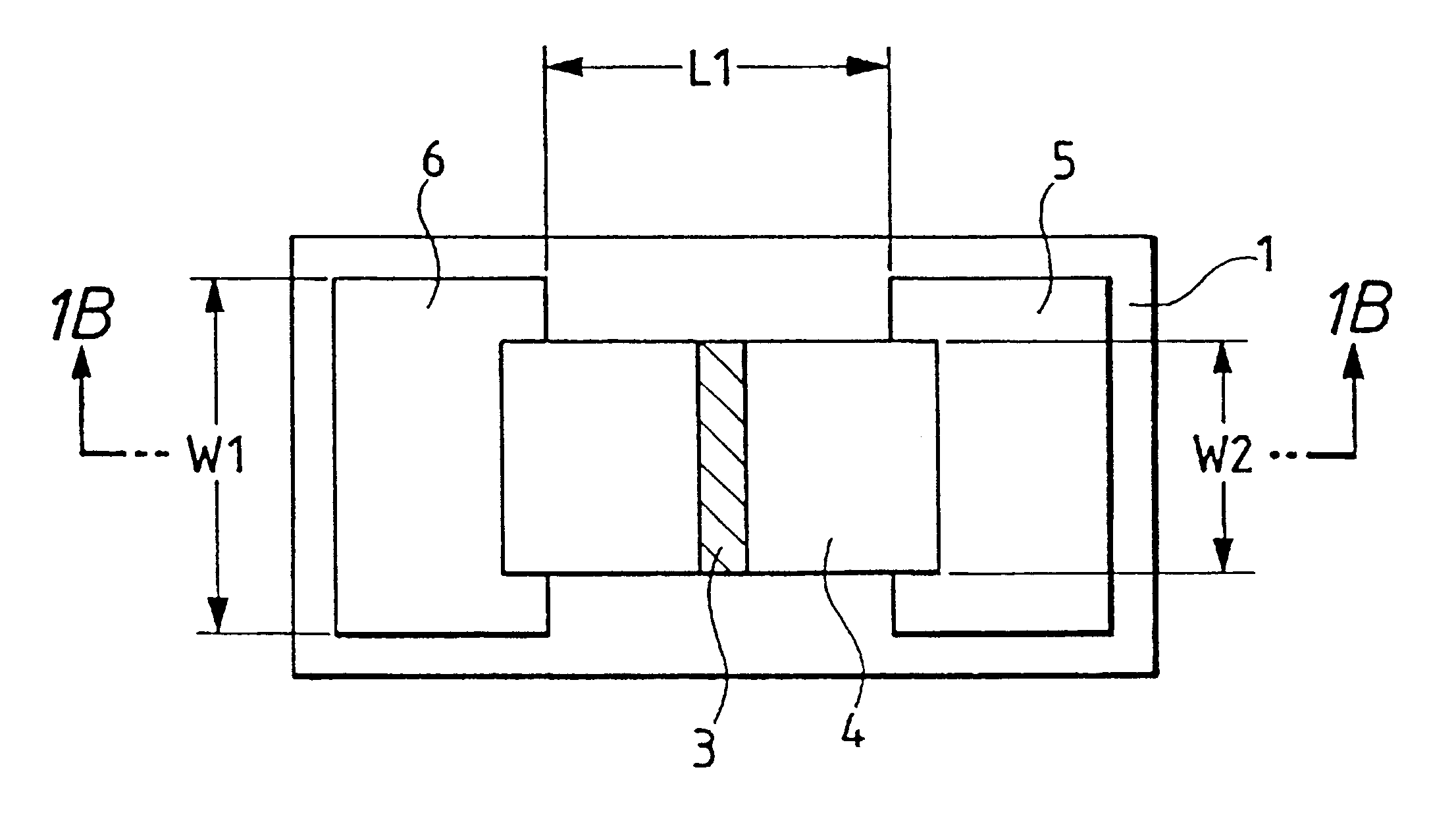
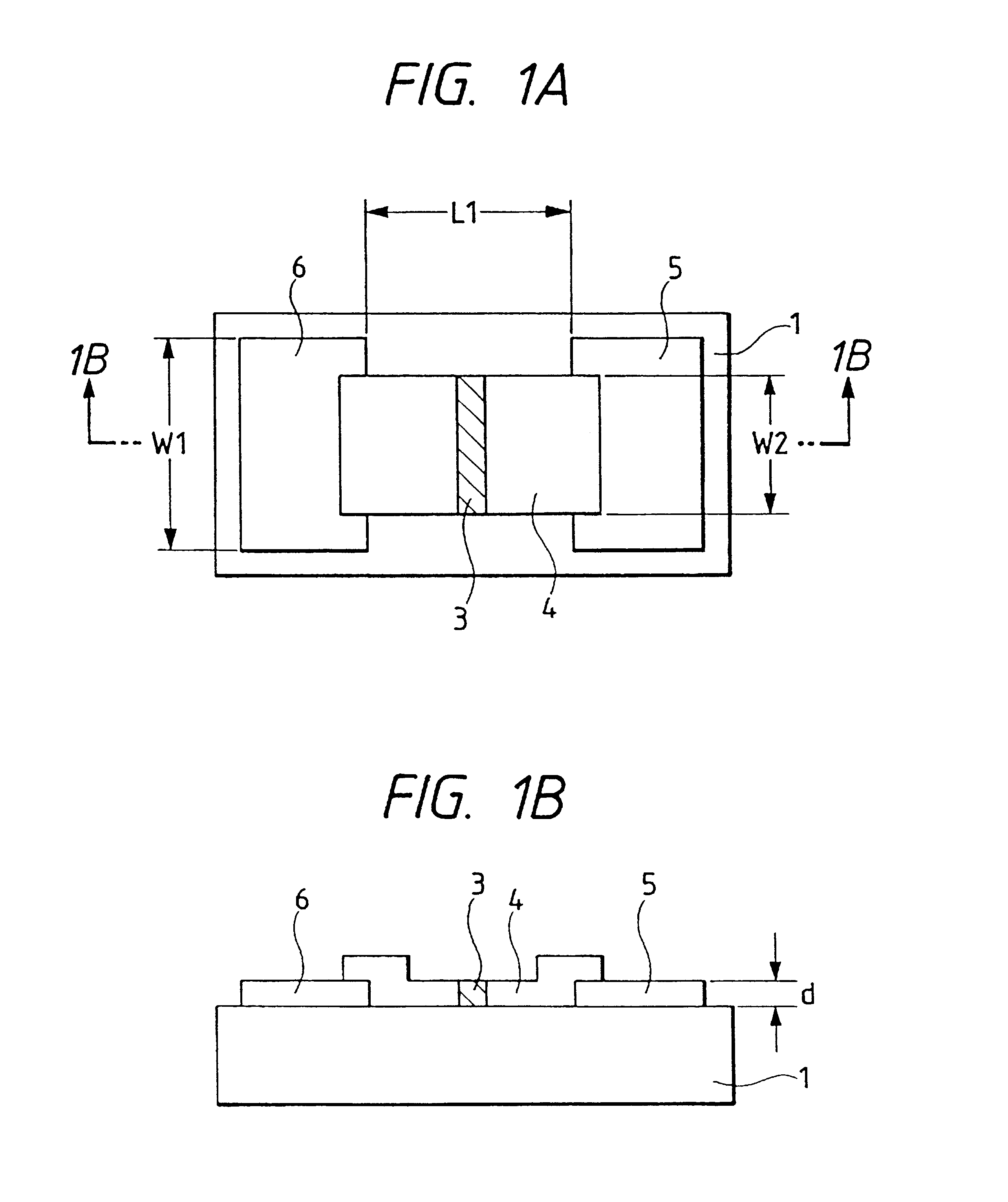
As an electron-emitting device of this Example, an electron-emitting device of the type shown in FIGS. 1A and 1B was fabricated. FIGS. 1A and 1B are respectively a plan and sectional views of the device. In FIGS. 1A and 1B, denoted by reference numeral 1 is an insulating base plate, 5 and 6 are device electrodes for applying a voltage to the device, 4 is a thin film including an electron-emitting region, and 3 is an electron-emitting region. Additionally, in FIGS. 1A and 1B, L1 represents the spacing between the device electrodes 5 and 6, W1 the width of the device electrodes, d the thickness of the device electrodes, and W2 the width of the device.
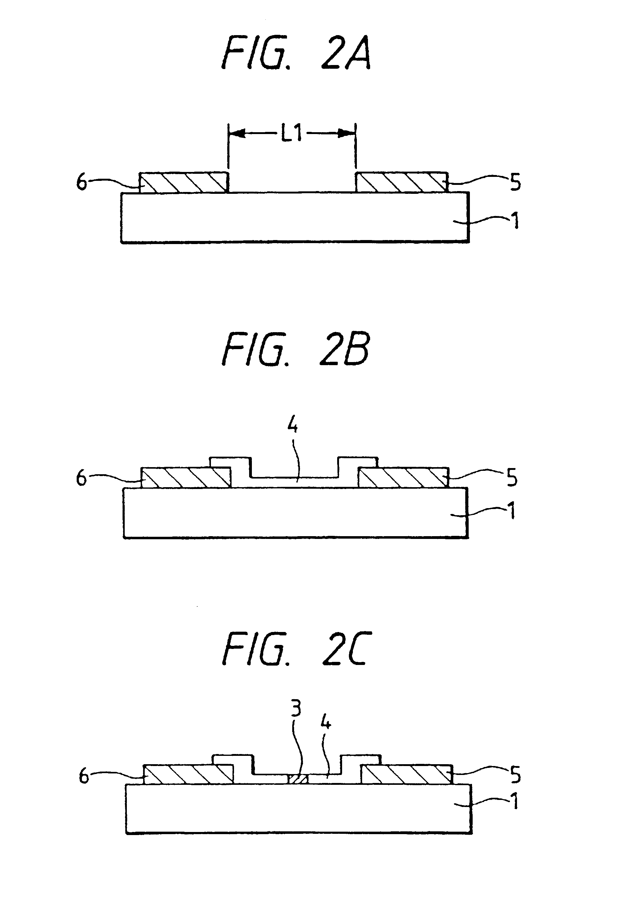
The manufacture process of the electron-emitting device of this embodiment will be described below with reference to FIGS. 2A to 2C.
A quartz plate was used as the insulating base plate 1 and, after sufficiently washing it with an organic solvent, the device electrodes 5, 6 made of Ni were formed on the surface of the base plate 1 (FIG. 2A...
example 2
In a similar manufacture process of electron-emitting devices as in above Example 1, a coating solution was prepared by dissolving, as an organic metal compound, 0.01 mol (2.488 g) of nickel acetate (4 hydrates) in 100 ml of water. The coating solution was coated on the insulating base plate 1 including the device electrodes 5, 6 formed thereon by using a spinner. The base plate was then heated to 350.degree. C., causing the organic metal compound to be decomposed and deposited on the base plate to form a fine particle film comprising nickel oxide fine particles (average size: 60 angstroms), thereby producing an electron-emitting region-forming thin film 2 (FIG. 2B). It was confirmed by X-ray analysis that the fine particles were made of nickel oxide.
example 3
A coating solution was prepared by dissolving, as an organic metal compound, 0.01 mol (2.249 g) of palladium acetate in 1000 ml of butyl acetate. The coating solution was coated on the insulating base plate 1 including the device electrodes 5, 6 formed thereon by using a spinner made by Mikasa Co. Ltd. at 1000 rpm for 30 seconds.
As a result of X-ray analysis (XD) of the coated film in this Example, it was confirmed that the diffraction patterns of Pd acetate observed in X-ray analysis (powder XD) was not found and the coated film had no crystallinity.
The base plate was then heated to 300.degree. C. inside an oven in an atmosphere of air, causing the organic metal compound to be decomposed and deposited on the base plate to form a fine particle film comprising palladium oxide fine particles (average size: 75 angstroms), thereby producing an electron-emitting region-forming thin film 2 (FIG. 2B).
PUM
| Property | Measurement | Unit |
|---|---|---|
| width | aaaaa | aaaaa |
| width | aaaaa | aaaaa |
| heat-resisting temperatures | aaaaa | aaaaa |
Abstract
Description
Claims
Application Information