

Conductive isostructural compounds
a technology of isostructural compounds and conductive materials, which is applied in the direction of optical radiation measurement, crystal growth process, solid-state devices, etc., can solve the problems of changing the composition of materials, allowing for fine adjustment of band gaps, and many current semiconductor materials are limited. , to achieve the effect of low thermal conductivity and wide range of electrical conductivity
- Summary
- Abstract
- Description
- Claims
- Application Information
AI Technical Summary
Benefits of technology
Problems solved by technology
Method used
Image

Examples
Embodiment Construction
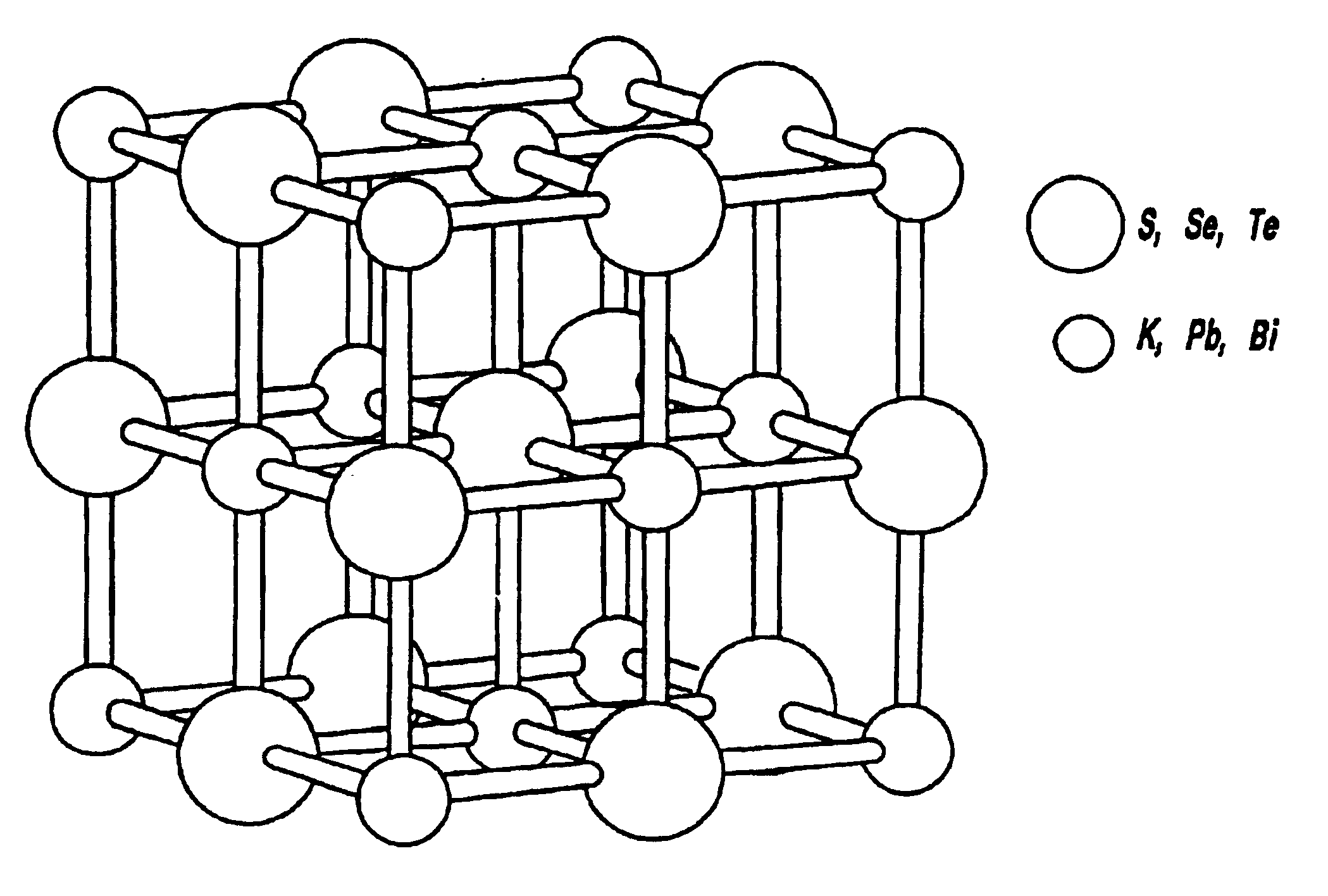
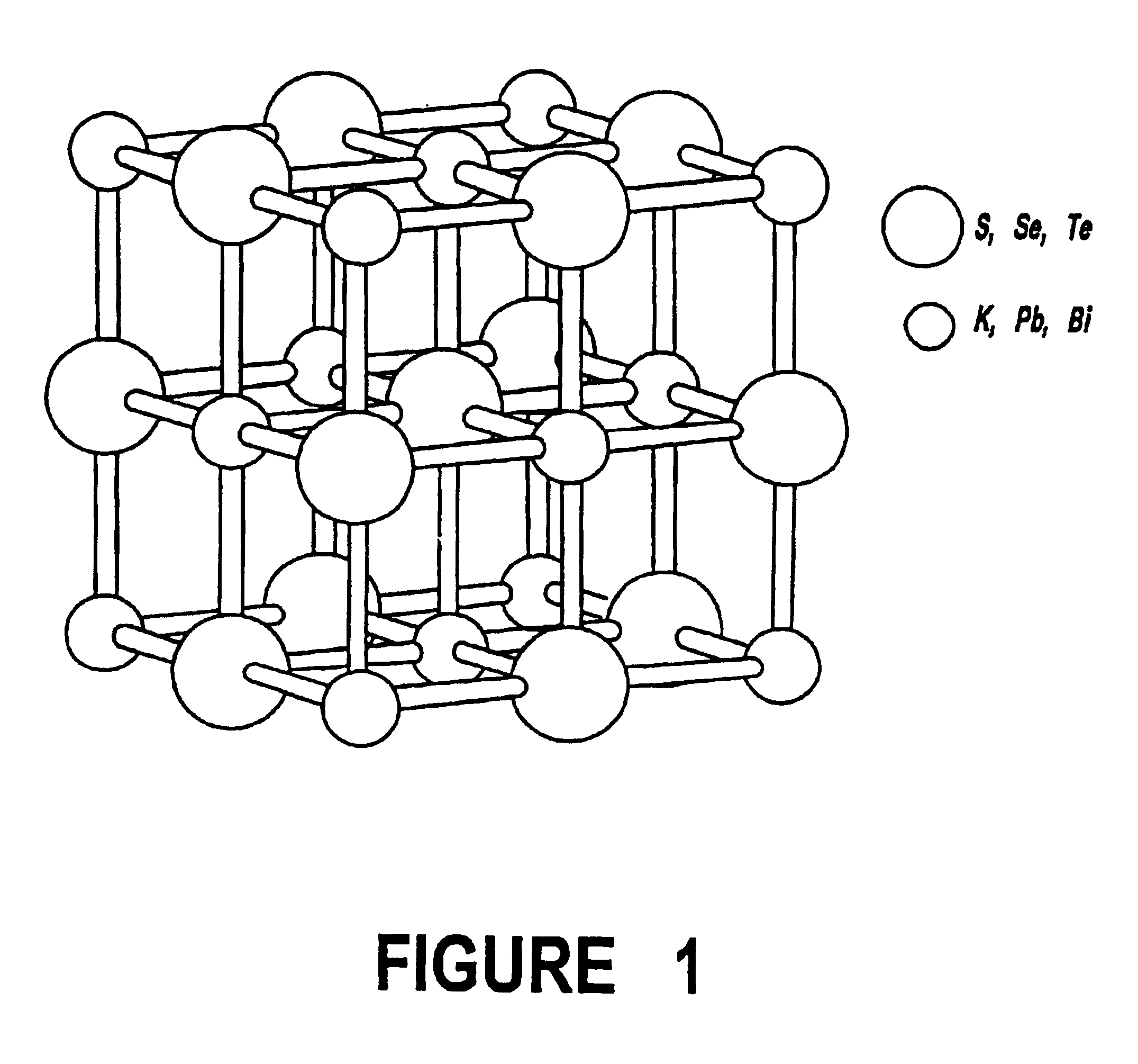
[0021]The present invention provides new isostructural compounds having the general formula AnMmM′nO2n+m where A is an alkali metal, such as lithium (Li), sodium (Na), potassium (K), rubidium (Rb), cesium (Cs) or the transition metals silver (Ag) or thallium (TI) and mixtures thereof, M is lead (Pb), tin (Sn), germanium (Ge), calcium (Ca), strontium (Sr), barium (Ba), any divalent transition metal or mixtures thereof, M′ is bismuth (Bi), antimony (Sb) or mixtures thereof, and Q is sulfur (S), selenium (Se), or tellurium (Te) and mixtures thereof.
[0022]The variables n and m can be any number greater than zero. Preferably, n and m are integers. While the variables n and m can theoretically be any integer, preferably, n and m are between 1 and 20. Additionally, the ratio of cations to anions present in the compounds of the present invention will preferably be 1:1.
[0023]The compounds of the present invention can be synthesized utilizing at least two different groups of starting material...
PUM
| Property | Measurement | Unit |
|---|---|---|
| residual pressure | aaaaa | aaaaa |
| temperature | aaaaa | aaaaa |
| temperature | aaaaa | aaaaa |
Abstract
Description
Claims
Application Information