Organic electro luminescence device and its manufacturing method
An electroluminescent device, organic technology, applied in the direction of electroluminescent light source, electro-solid device, semiconductor/solid-state device manufacturing, etc., can solve the problem of not being able to ensure the uniformity of organic functional layer evaporation at the same time, adverse device overall performance and yield It can not significantly improve the contrast of the device and other problems, so as to achieve the effect of saving equipment investment costs, saving production management costs, and improving life expectancy.
- Summary
- Abstract
- Description
- Claims
- Application Information
AI Technical Summary
Problems solved by technology
Method used
Image

Examples
Embodiment 1
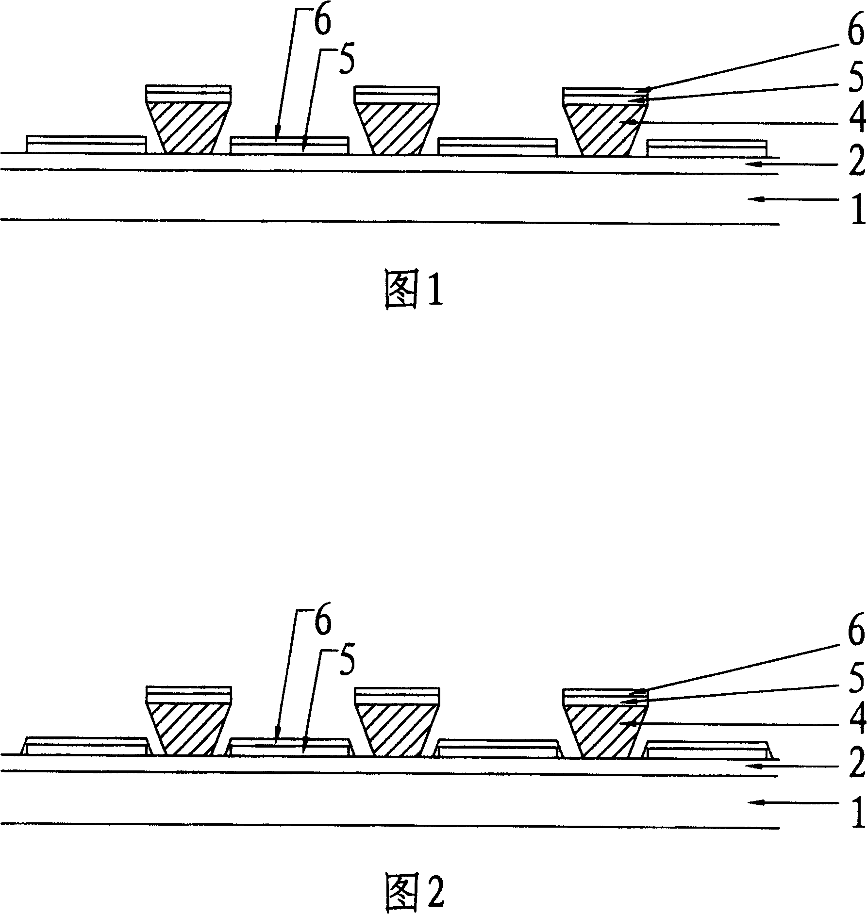
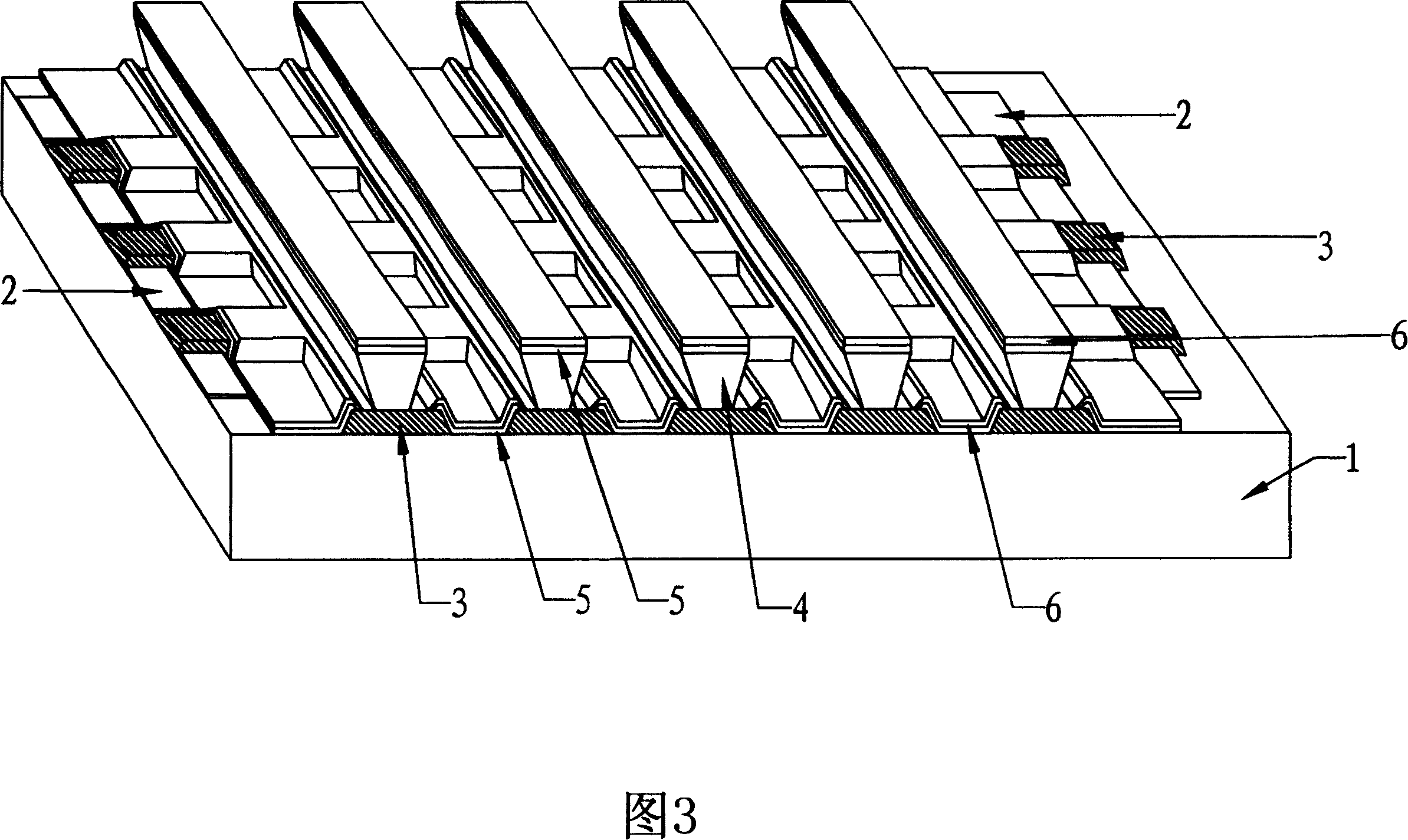
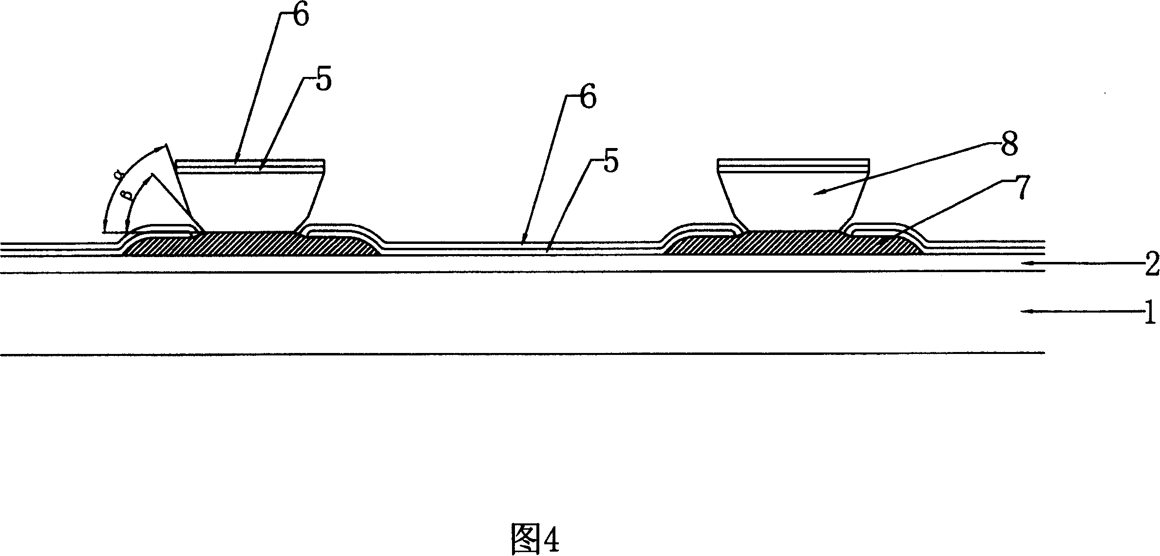
[0069] (The entire preparation process of OLED is carried out in the purification workshop.) ITO glass with a square resistance of 10Ω is cleaned with UV irradiation and lotion containing surfactant in sequence, and then dried. The film thickness of ITO is 180nm. A group of parallel and separated straight lines are engraved with a line width of 100 μm and a line gap of 15 μm. After cleaning and drying again, the first layer of negative cyclized rubber, an organic insulating material, was spin-coated on the ITO pattern with a film thickness of 1.1 μm, and baked on a hot plate at 100°C for 90s. The first layer is exposed but not developed, and the exposure pattern is a network structure, that is, only the light-emitting area and the lead connection area of the pixel point of the device are exposed. The line width parallel to the ITO line is 30 μm, and the line perpendicular to the ITO line The width is 30 μm. Then continue to spin-coat the second layer of insulating material ...
Embodiment 2
[0071] (The entire preparation process of OLED is carried out in the purification workshop.) ITO glass with a sheet resistance of 15Ω is cleaned and dried with UV irradiation and lotion containing surfactant in sequence. The film thickness of ITO is 170nm. A group of parallel and separated straight lines were produced, with a line width of 400 μm and a line gap of 30 μm. After cleaning and drying again, the first layer of organic insulating material photosensitive PI DL-1000 was spin-coated on the ITO pattern with a film thickness of 1.5 μm, and baked in a convection oven at 125°C for 25 minutes. The first layer is exposed but not developed, and the exposure pattern is a network structure, that is, only the light-emitting area and the lead connection area of the pixel point of the device are exposed. The line width parallel to the ITO line is 45 μm, and the line perpendicular to the ITO line The width is 40 μm. Then continue to spin-coat the second layer of insulating mater...
Embodiment 3
[0073] (The entire preparation process of OLED is carried out in the purification workshop.) ITO glass with square resistance -4 Evaporate organic functional layers and metal layers in a vacuum furnace above Pa. The organic functional layer is sequentially composed of CuPc, NPB and Alq 3 Composition, the film thickness is 20nm, 70nm and 50nm respectively. The metal layer is sequentially composed of Mg:Ag alloy (evaporation rate ratio 10:1, alloy mass ratio 4:1) and Ag, and the film thicknesses are 100nm and 300nm respectively. Encapsulate the device in an inert atmosphere. The lighting voltage of the device is 2.7V, the light is uniform, and the current density is 20mA / cm 2 The luminous efficiency is 4.51m / W, and the device life is more than 5000
PUM
| Property | Measurement | Unit |
|---|---|---|
| Luminous efficiency | aaaaa | aaaaa |
Abstract
Description
Claims
Application Information
 - Generate Ideas
- Intellectual Property
- Life Sciences
- Materials
- Tech Scout
- Unparalleled Data Quality
- Higher Quality Content
- 60% Fewer Hallucinations
Browse by: Latest US Patents, China's latest patents, Technical Efficacy Thesaurus, Application Domain, Technology Topic, Popular Technical Reports.
© 2025 PatSnap. All rights reserved.Legal|Privacy policy|Modern Slavery Act Transparency Statement|Sitemap|About US| Contact US: help@patsnap.com