Epitaxial thin films

An epitaxial thin film and thin film technology, applied in the field of epitaxial thin films of dielectric materials

Inactive Publication Date: 2008-04-30
MICROCOATING TECH
View PDF13 Cites 0 Cited by
  • Summary
  • Abstract
  • Description
  • Claims
  • Application Information

AI Technical Summary

Problems solved by technology

But this deposition method requires va...

Method used


Image

  • Epitaxial thin films
  • Epitaxial thin films
  • Epitaxial thin films

Examples


Embodiment 1

[0050] In this example, the SrTiO 3 (STO) deposited on rolled textured nickel. The precursor solution included 1.26 g strontium 2-ethylhexanoate (2eh) (diluted with toluene to 1.5 wt.% strontium), 1.11 g titanium diisopropoxybisacetylacetonate (diluted to 0.94 wt. %), 51ml denatured ethanol and 300g propane. The solution was added to the needle at a rate of 3 ml / min while a heating current of 1.75A was applied to the needle. Nozzle oxygen at 3 lpm at 80 psi, hydrogen pilot gas at 15 psi at 18 lpm, and argon at 32 lpm at 50 psi as shielding gas. Deposition was carried out for 10 minutes at a substrate temperature of 950°C.

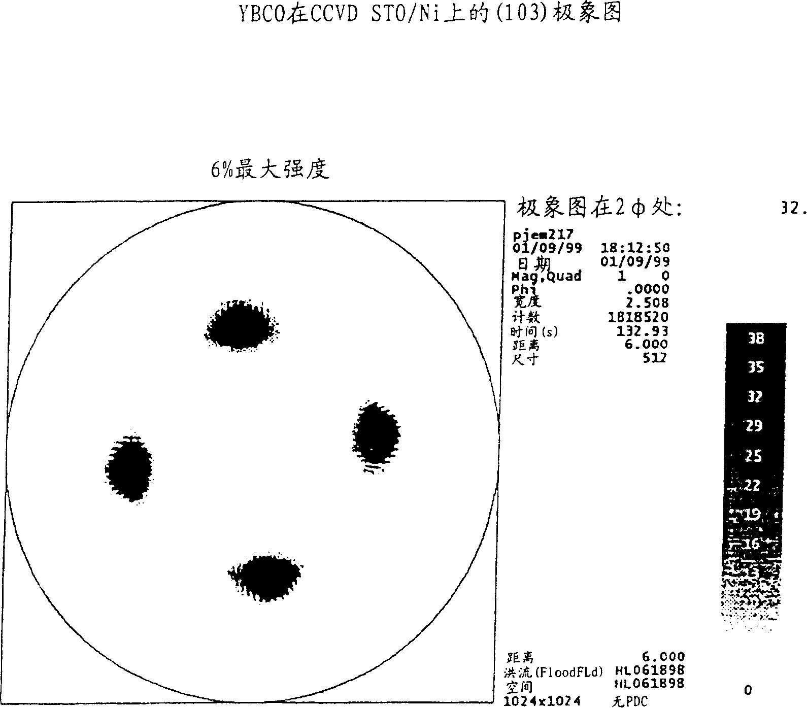
[0051] Such as image 3 As shown, the deposited buffer layer is highly epitaxial, exhibiting a single cubic in-plane orientation. image 3 is SrTiO deposited on nickel by CCVD 3 YBa deposited on the surface of the buffer layer 2 Cu 3 o x Pole image diagram of (YBCO) superconductor. The polar image of the YBCO layer exhibits the same uniplane in-pl...

Embodiment 2

[0061] In this example, LSM was deposited on a-plane sapphire using CCVD. The precursor solution included 0.21g Mn-2eh (diluted to 6% by weight of Mn with mineral spirits), 1.96g of La-2eh (diluted to 2% by weight of La with mineral spirits), 0.97g of Sr-2eh (10% by weight of %Sr in 2-ethylhexanoic acid, further diluted with toluene to a Sr of 1.25% by weight). This solution was added to toluene to make a total volume of 10 ml, then added to 60 g of propane. The solution was added at a rate of 3 ml / min for a total deposition time of 30 minutes. A 2.42A current was applied to the needle, and the nozzle oxygen flow rate was 3500ml / min. The nozzle oxygen pressure is 60 psi (no hydrogen or argon). The flame temperature is maintained at 1200-1400°C. exist Figure 8 , SEM micrographs of LSM on sapphire showing a porous and columnar microstructure. The electrode layer must have sufficient porosity to transport gaseous species or ions to the electrolyte while collecting electron...

Embodiment 3

[0063] In this example, YSB was deposited on a-plane sapphire by CCVD. The precursor solution included 2.88g Ba-2eh (8.5 wt% Ba in xylene, further diluted with toluene to 2 wt% Ba), 0.08g Y-2eh (diluted to 0.69 wt% Y with toluene). This solution was added to toluene to make a total volume of 10 ml, then added to 60 g of propane. The solution was added at a rate of 3 ml / min for a total deposition time of 29 minutes. A current of 2.50A was applied to the needle, and the nozzle oxygen flow rate was 3300ml / min. The flame temperature was maintained at 1200°C. The nozzle oxygen pressure is 60 psi (no hydrogen or argon).


PUM

PropertyMeasurementUnit
Thicknessaaaaaaaaaa

Abstract

Epitaxial thin films for use as buffer layers for high temperature superconductors, electrolytes in solid oxide fuel cells (SOFC), gas separation membranes or dielectric material in electronic devices, are disclosed. By using CCVD, CACVD or any other suitable deposition process, epitaxial films having pore-free, ideal grain boundaries, and dense structure can be formed. Several different types of materials are disclosed for use as buffer layers in high temperature superconductors. In addition, the use of epitaxial thin films for electrolytes and electrode formation in SOFCs results in densification for pore-free and ideal grain boundary/interface microstructure. Gas separation membranes for the production of oxygen and hydrogen are also disclosed. These semipermeable membranes are formed by high-quality, dense, gas-tight, pinhole free sub-micro scale layers of mixed-conducting oxides on porous ceramic substrates. Epitaxial thin films as dielectric material in capacitors are also taught herein. Capacitors are utilized according to their capacitance values which are dependent on their physical structure and dielectric permittivity. The epitaxial thin films of the current invention form low-loss dielectric layers with extremely high permittivity. This high permittivity allows for the formation of capacitors that can have their capacitance adjusted by applying a DC bias between their electrodes.

Description

[0001] government contract [0002] Rights in this invention are vested in the United States Government under Contract Nos. F33615-98-C-5418 of the Department of Defense, Contract Nos. DE-FG02-97ER82345, ACQ-9-29612-01, and 4500011833 of the United States Department of Energy. [0003] related application [0004] This application claims priority to US Provisional Patent Application No. 60 / 115,519, filed January 12, 1999, which is hereby incorporated by reference in its entirety. field of invention [0005] The present invention relates to epitaxial thin films, and more particularly, the present invention relates to epitaxial thin films useful especially as buffer layers for high temperature superconductors, electrolytes for solid oxide fuel cells (SOFCs), gas separation membranes, or dielectric materials for electronic components. background of the invention [0006] Although it has been demonstrated in the past to deposit epitaxial coatings on textured substrates, the ...

Claims


Application Information

Patent Timeline
IPC IPC(8): H01L39/24H01M8/02H01G4/06B01D71/02C30B29/22H01BH01B1/00H01G4/33H01L21/20H01L49/02
CPCH01L39/2461H10N60/0632
Inventor A·T·亨特G·德什潘德D·T·-J·J·卡振斯W·-Y·林S·S·肖普
Owner MICROCOATING TECH
Why Eureka
Try Eureka