Nuclear radiation detector and producing technology thereof
A nuclear radiation detector and manufacturing process technology, applied in the field of nuclear radiation detectors, can solve problems such as inability to realize simultaneous measurement, poor long-term stability, poor energy resolution, etc., and achieve excellent electrical characteristics and detection characteristics, and excellent energy resolution The effect of high rate and good position resolution
- Summary
- Abstract
- Description
- Claims
- Application Information
AI Technical Summary
Problems solved by technology
Method used
Image
Examples
Embodiment 1
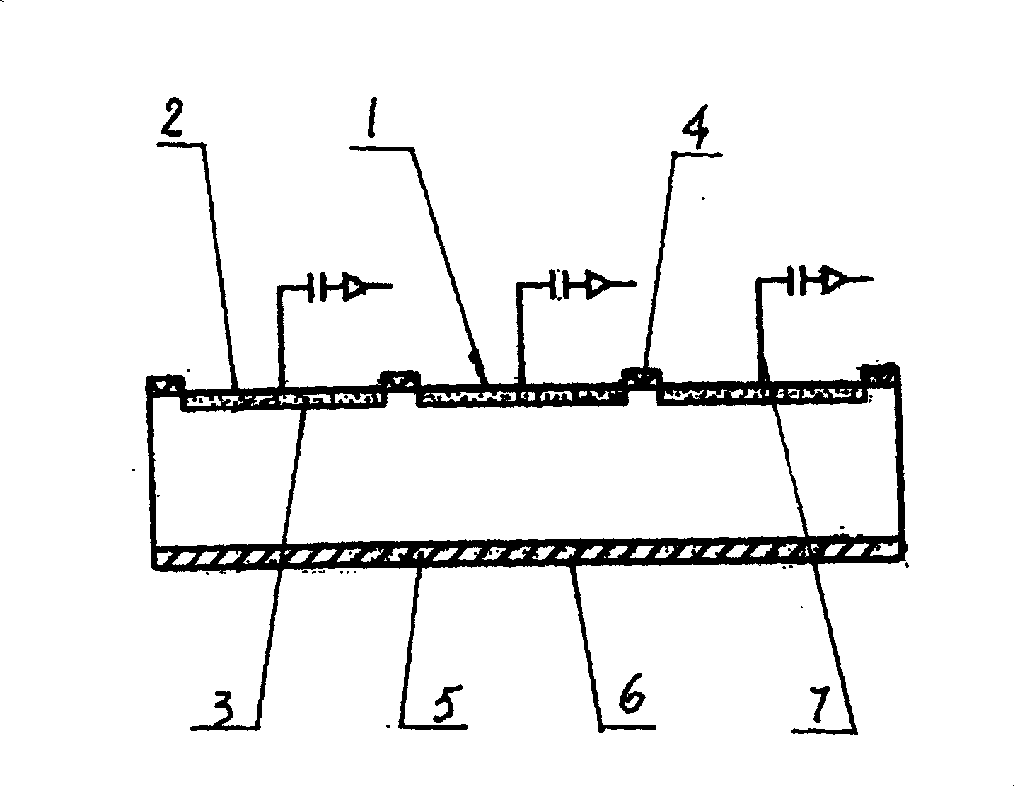
[0032] Example 1: see figure 1 , nuclear radiation detector, the effective area is 50×20mm 2 Silicon substrate, N type, detection window 1 is composed of 16 detection windows 1 parallel to each other, each silicon strip is 3mm wide, 20mm long, with B + The doped region 3 forms a PN junction, on which there is an Al layer 2 and a lead 7 is provided; between the two detection windows 1 there is SiO 2 Divider 4, SiO 2 The width of the division area is 140μm; there are P on the back of the silicon substrate - doped region 5, forming N + An ohmic contact, on which an Al layer 6 forms the back electrode. The resistivity of the silicon substrate is 8000-12000 Ω·cm, the thickness is 300 μm, the crystal orientation [111], the charge carrier lifetime is 1-3 ms, and there is no dislocation. The lead wire 7 is connected to the radio frequency cable socket.
Embodiment 2
[0033] Embodiment 2: The manufacturing process of nuclear radiation detector:
[0034] A. Surface oxidation passivation: use N-type silicon wafers, after cleaning, generate 7000 When the surface is oxidized and passivated, the atmosphere of chloride ions is brought in by nitrogen through trichlorethylene liquid, the flow rate is 0.2 liters / minute, the flow rate of oxygen is 6 liters / minute, and the temperature is 950 ° C ~ 1050 ° C .
[0035] B. Photolithographic detector detection window 1 .
[0036] C. Ion implantation: implant B on the detector detection window 1 side + ions, the implanted ion concentration is 5×10 13 / cm 2 -1×10 14 / cm 2 .
[0037] D. Remove the SiO on the back of the silicon substrate 2 layer, injected into P - Phosphorus ion concentration is 5×10 15 / cm 2 -1×10 16 / cm 2 . P -Doped region 5 forms N + The thickness of the layer is 1.5 to 2.0 μm.
[0038] E. After ion implantation, anneal to form PN junction and N + Ohmic contact, the ann...
PUM
 Abstract
Description
Claims
Application Information
