

High depth-width ratio deep sub-micrometer, nanometer metal structure making process based on self-supporting thin film
A self-supporting thin film, deep submicron technology, applied in nanostructure manufacturing, photoengraving process of pattern surface, nanotechnology, etc. It is difficult to achieve and other problems to achieve the effect of strong practical value
- Summary
- Abstract
- Description
- Claims
- Application Information
AI Technical Summary
Problems solved by technology
Method used
Image

Examples
Embodiment
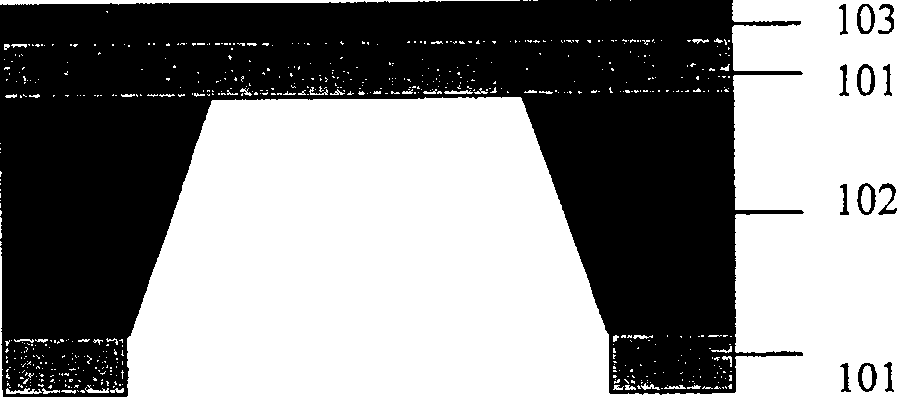
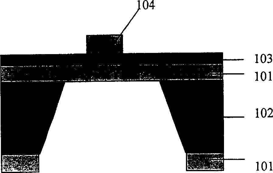
[0033] 1. If Figure 2-1 As shown, firstly, a thin chromium and thin gold layer 203 is deposited on the front surface of the Π-shaped self-supporting film. The thin chromium and thin gold layer 203 can be obtained by electron beam evaporation, with a total thickness of 10-30 nm. The Π-shaped self-supporting film is composed of a silicon nitride film 101 and a silicon chip 102, the bottom leg is a silicon nitride film 101, the middle leg is a silicon chip 102, and the upper end is a silicon nitride film 101.
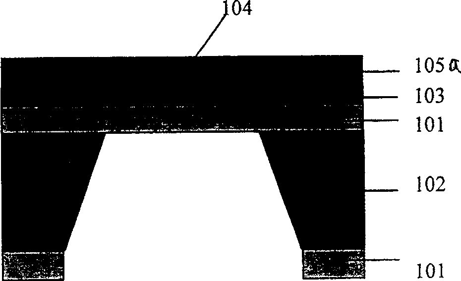
[0034] 2. If Figure 2-2 As shown, the electron beam glue 204 is thrown on the surface of the thin chrome and thin gold layer 203. The thickness of the electron beam glue 204 is 150-600nm, and the pre-baking is performed with a hot plate. The pre-baking temperature is 105° C. and the pre-baking time is 2 minutes.
[0035] 3. Figure 2-3 As shown, electron beam exposure is carried out on the electron beam glue 204, the dose is 35 microcoulombs, and then the electron beam...
PUM
| Property | Measurement | Unit |
|---|---|---|
| thickness | aaaaa | aaaaa |
| thickness | aaaaa | aaaaa |
| thickness | aaaaa | aaaaa |
Abstract
Description
Claims
Application Information