Manufacturing method of semiconductor

A manufacturing method and semiconductor technology, applied in semiconductor/solid-state device manufacturing, electrical components, circuits, etc., can solve problems such as lower pass rate of DARM products and surface damage of Si substrates

Inactive Publication Date: 2009-03-04
SEMICON MFG INT (SHANGHAI) CORP +1
View PDF4 Cites 0 Cited by
  • Summary
  • Abstract
  • Description
  • Claims
  • Application Information

AI Technical Summary

Problems solved by technology

[0004] The electrical insulating isolation layer set between adjacent source regions is usually etched on a Lam Exelan machine. Due to the characteristics of the Exelan dual-frequency plasma source used, the plasma damages the surface of the Si substrate, resulting in source region insulation. The pass rate of DARM products of the isolation layer is reduced

Method used


Image

  • Manufacturing method of semiconductor

Examples


Embodiment Construction

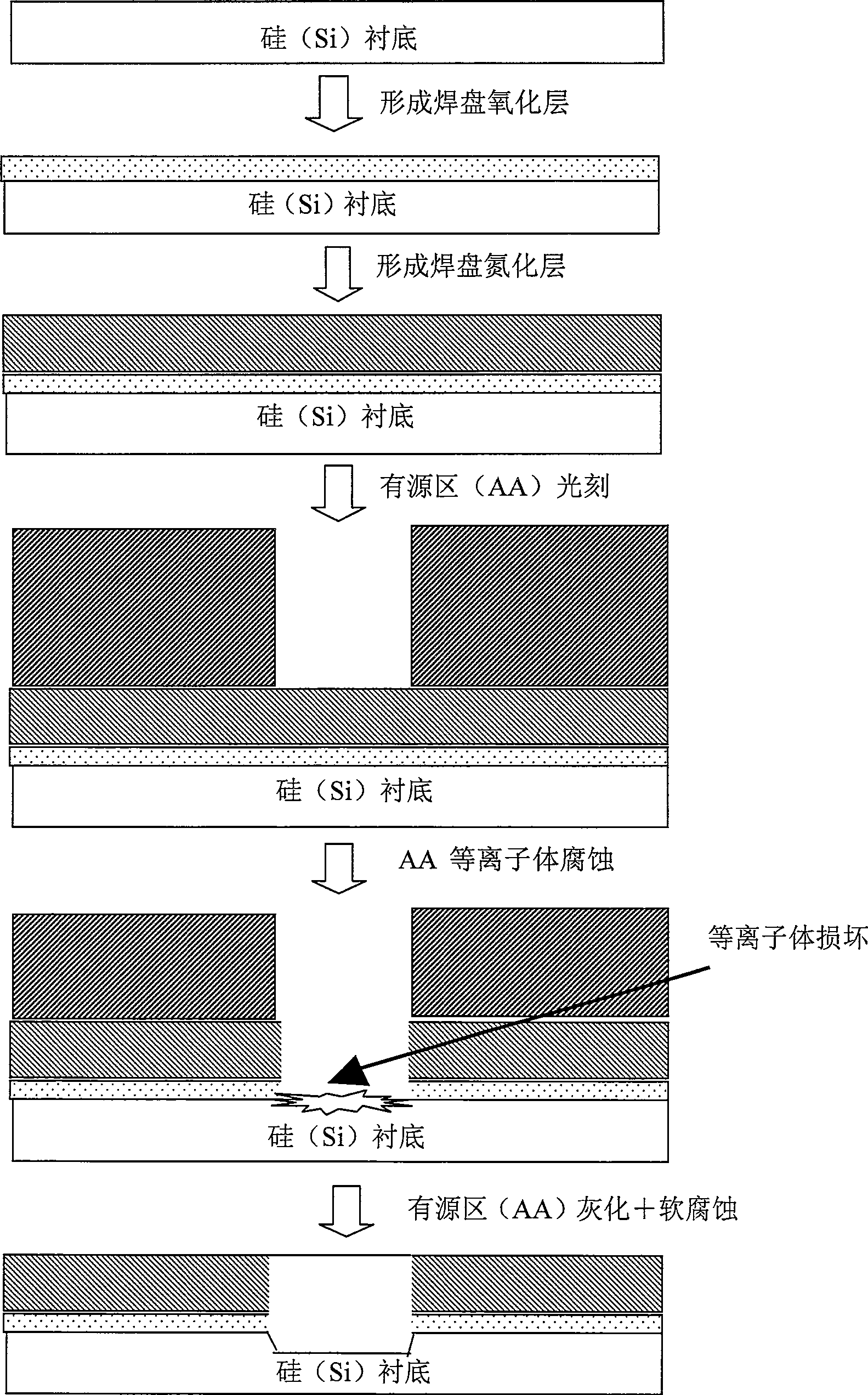
[0016] According to the manufacturing method of semiconductor device of the present invention, comprise the following steps:

[0017] Step 1: grow pad oxide layer (Pad-ox) by diffusion furnace on Si substrate, its thickness is

[0018] Step 2: Then grow silicon nitride (Si 3 N 4 ) (its thickness is ).

[0019] Step 3: Add photoresist (PR) on the insulating film to form the isolation layer, and use a mask with an isolation layer pattern for exposure and development

[0020] Step 4: active area etching (RIE plasma etching);

[0021] Step 5: Additional soft corrosion, soft corrosion is a kind of physical and chemical corrosion, under microwave plasma (frequency 2.45GHz), use CF 4 / O 2 The mixed gas used as an etchant to remove lattice defects caused by plasma damage, CF 4 / O 2 The flow rate ratio of the mixed gas is CF 4 :O 2 =1:(3~5), preferred CF 4 / O 2 The flow rate ratio of the mixed gas is CF 4 :O 2 =1:4.

[0022] Step 6: stripping the photoresist (PR);

...


PUM


Abstract

This invention puts forward a manufacturing method for semiconductor devices, especially DRAM, which adds an attached soft corrosion process to the source trap insulation layer after being corroded and takes a mixed gas of CE4 / O2 as the corroding gas under the microwave state with the frequency of 2.45GHz to eliminate the lattice defect caused by the harm of plasmas on a silicon substrate surface by the chemical reaction of corroding gas on the silicon substrate surface so as to ensure to constitute DRAM products with qualified electric property.

Description

technical field [0001] The manufacturing method of the semiconductor device that the present invention relates to especially relates to the method of adding soft etching after etching the source isolation layer of dynamic random access memory (hereinafter referred to as DRAM) to remove plasma damage and improve refresh time. Background technique [0002] With the increasing integration of integrated circuits and the continuous improvement of integrated circuit manufacturing technology, the patterning line width of integrated circuits has become smaller and smaller. The influence of continuity is also increasing, so the influence on the electrical properties of semiconductor devices is becoming more and more obvious. In particular, lattice defects caused by plasma damage on the surface of the silicon substrate are increasingly damaging the electrical properties of DRAM products, and may even lead to failure of the entire DRAM product or the entire integrated circuit. [0003...

Claims


Application Information

Patent Timeline
Patent Type & Authority Patents(China)
IPC IPC(8): H01L21/76H01L21/314H01L21/3065H01L21/8242
Inventor 吴长明蒋晓钧黄光瑜徐立
Owner SEMICON MFG INT (SHANGHAI) CORP
Why Eureka
Try Eureka