Method for preparing transistor T type nano grid

A transistor and nanotechnology, applied in semiconductor devices, semiconductor/solid-state device manufacturing, electrical components, etc., can solve the problems of poor adhesion, difficult to remove electron beam glue, affecting the exposure and development of gate feet, and achieve electron beam exposure. And the development conditions are loose, the development time is easy to control, and the development is easy to control.

Active Publication Date: 2009-09-23
SEMICON MFG INT (SHANGHAI) CORP +1
View PDF2 Cites 0 Cited by
  • Summary
  • Abstract
  • Description
  • Claims
  • Application Information

AI Technical Summary

Problems solved by technology

Since the first layer and the third layer of electron beam glue used to define the grid cap and grid foot are both ZEP520A glue, their sensitivity to electron beam exposure is consistent. Therefore, this process has very strict requirements on the selection of the dose of two electron beam exposures and the control of the development conditions, and the process is difficult to realize.
[0009] In addition, due to the poor adhesion between ZEP520A and the epitaxial wafer, a layer of dielectric needs to be deposited before evenly coating the glue. The dielectric is usually silicon nitride or silicon dioxide. After exposure and development, the dielectric at the gate groove must be etched Etching, the etching of nanometer-sized thin lines is difficult to control, the process is difficult, and the underlying ZEP520A electron beam glue is difficult to remove, which is easy to affect the characteristics of the device

Method used


Image

  • Method for preparing transistor T type nano grid
  • Method for preparing transistor T type nano grid
  • Method for preparing transistor T type nano grid

Examples


Embodiment

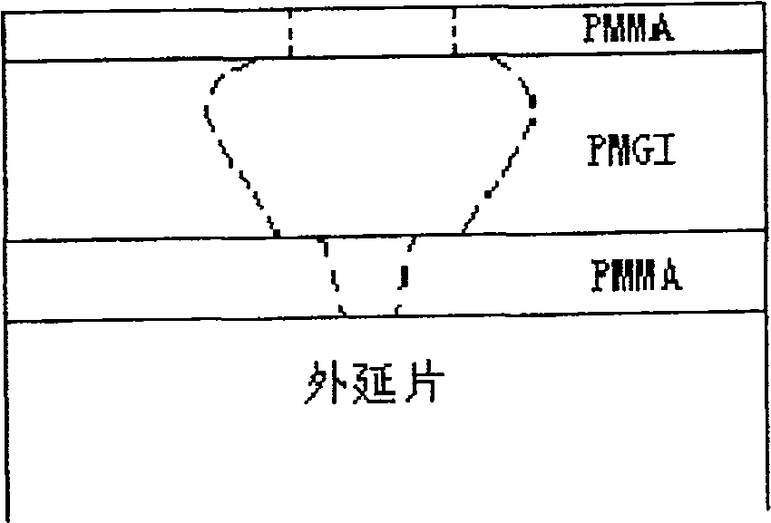
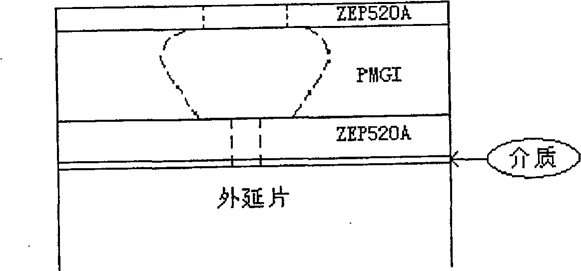
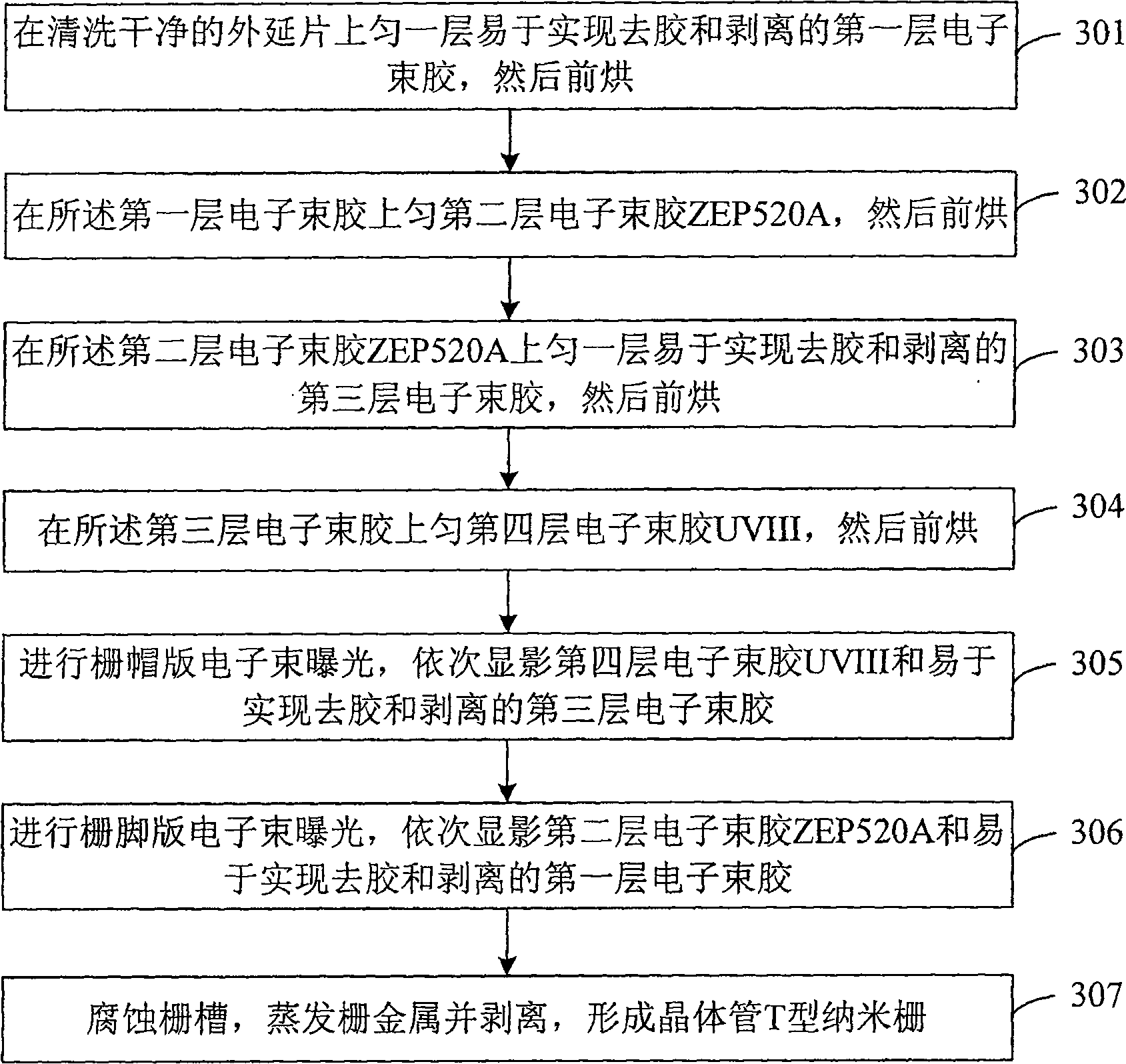
[0069] In this embodiment, the method for fabricating a high electron mobility transistor (HEMT) T-type nano-gate is aimed at some shortcomings in the current fabrication of a high electron mobility transistor (HEMT) T-type nano-gate. PMGI / ZEP520A / PMGI / UVIII four layers The electron beam photoresist structure (shown in Table 1) and two electron beam exposure methods were used to fabricate high electron mobility transistor (HEMT) T-type nano gates.

[0070] Table 1 is a schematic diagram of the PMGI / ZEP520A / PMGI / UVIII four-layer electron beam photoresist structure used in the method for fabricating a high electron mobility transistor (HEMT) T-type nano gate according to the present invention:

[0071]

[0072] Table 1

[0073] In this embodiment, the first layer of electron beam glue and the third layer of electron beam glue, which are easy to achieve stripping and stripping, are PMGI electron beam glue, which is used in the method of fabricating high electron mobility transistor...


PUM


Abstract

The invention discloses a method for manufacturing transistor T-shaped nanometer gate, comprising the steps of: A, coating a first layer electric beam glue which is liable to realize glue-stripping and peeling on a cleaned epitaxial wafer, and then soft-baking; B, coating a second layer electric beam glue ZEP520A on the first layer electric beam glue, and then soft-baking; C, coating a third layer electric beam glue which is liable to realize glue-stripping and peeling on the second layer electric beam glue ZEP520A, and then soft-baking; D, coating a fourth layer electric beam glue UVIII on the third layer electric beam glue, and then soft-baking; E, carrying out gate cap electric beam exposure, and sequentially developing the four layer electric beam glue UVIII, the third layer electric beam glue which is liable to realize glue-stripping and peeling; F, carrying out the gate feet electric beam exposure, and sequentially developing the second layer electric beam glue ZEP520A and the first layer electric beam glue which is liable to realize glue-stripping and peeling; G, eroding the gate groove, evaporating and peeling off gate metals to form the transistor T-shaped nanometer gate. Usage of the invention can easily manufacture the gate lines having small size, greatly reducing the process difficulty.

Description

Technical field [0001] The invention relates to the technical field of compound semiconductors, in particular to a method for fabricating a transistor T-type nano gate with high electron mobility. Background technique [0002] The fabrication of the gate is the most critical process in the fabrication of high electron mobility transistor (HEMT) devices. Since the gate length directly determines the frequency, noise and other characteristics of the HEMT device, the smaller the gate length, the current cut-off frequency of the device (f T ) And power gain cutoff frequency (f max The higher the ), the smaller the noise figure of the device. People have continuously reduced the gate length of the high electron mobility transistor (HEMT) device to obtain devices with better characteristics. [0003] As the gate length is shortened, the gate resistance increases. When the gate length is reduced to less than 0.5 μm, the microwave loss of the gate resistance makes the gain attenuation mo...

Claims


Application Information

Patent Timeline
Patent Type & Authority Patents(China)
IPC IPC(8): H01L21/28H01L21/335
Inventor 刘亮张海英刘训春
Owner SEMICON MFG INT (SHANGHAI) CORP
Why Eureka
Try Eureka