

Wafer linking boride surface treating pigment as well as linking method
A surface treatment agent and wafer bonding technology, which is applied in the field of surface treatment agent for wafer bonding and boride surface treatment agent for wafer bonding. and other problems, to achieve the effect of high-strength bonding, short annealing time, and low bonding temperature
- Summary
- Abstract
- Description
- Claims
- Application Information
AI Technical Summary
Problems solved by technology
Method used
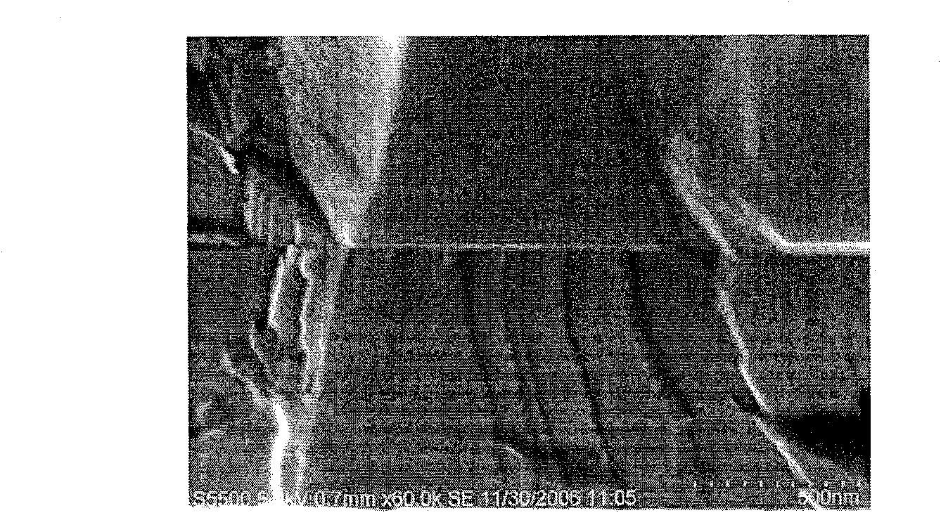
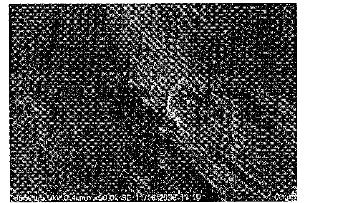
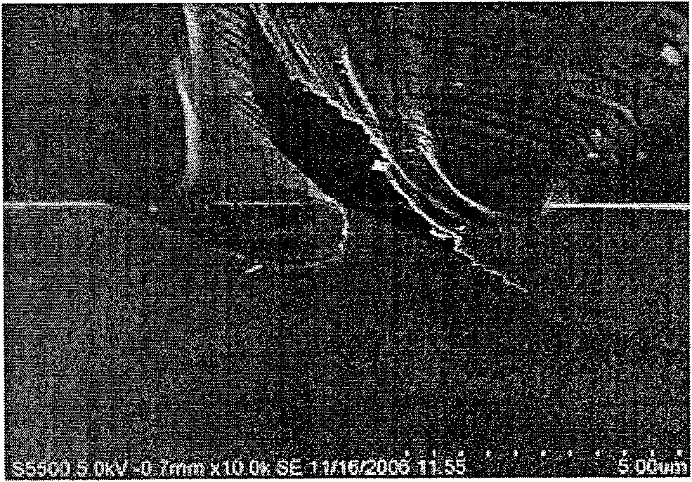
Image

Examples
Embodiment 1
[0031] Embodiment 1 (GaAs / InP bonding):
[0032] Clean the InP wafer and GaAs wafer to be bonded in acetone, ethanol, ammonia water and deionized water to remove surface stains;
[0033] Boric acid (H 3 BO 3 ) dissolved in ammonia (NH 4 OH), made into a saturated solution at room temperature, as a surface treatment agent;
[0034] Place the cleaned wafer in a surface treatment agent and place it at 99°C for 1 minute;
[0035] Take out the two wafers face to face, and clamp them with a clamp;
[0036]Put the clamped wafer and the clamp together into an annealing furnace for heat treatment, and keep it at a heat treatment temperature of 295°C for 0.5 hours to achieve high-strength bonding between the wafers.
Embodiment 2
[0037] Embodiment 2 (Si / InP bonding):
[0038] Clean the InP wafer to be bonded in acetone, ethanol, ammonia water and deionized water to remove surface stains;
[0039] Form an extremely thin layer of silicon oxide (about 10 nanometers thick) on the surface of the Si wafer to be bonded;
[0040] Si wafer with H 2 SO 4 :H 2 o 2 and HCl:H 2 o 2 :H 2 O solution cleaning to remove surface stains;
[0041] With 1% sodium borohydride (NaBH 4 ) aqueous solution, take 3ml of this solution (No. 1 solution); get 0.5ml of ammonia water (No. 2 solution); mix 1% boric acid (H 3 BO 3 ) aqueous solution, take 25ml of this solution (No. 3 solution); mix No. 1, 2, and 3 solutions to prepare a surface treatment agent;
[0042] Place the cleaned wafer in a surface treatment agent and place it at 60°C for 10 minutes;
[0043] Take out the two wafers face to face, and clamp them with a clamp;
[0044] Put the clamped wafer and the clamp together into an annealing furnace for heat tre...
Embodiment 3
[0045] Example 3 (Si / Si bonding):
[0046] Form a thin layer of silicon oxide (about 5 nanometers thick) on the surface of the Si wafer to be bonded;
[0047] Si wafer with H 2 SO 4 :H 2 o 2 and HCl:H 2 o 2 :H 2 O solution cleaning to remove surface stains;
[0048] Take 0.1g of sodium borohydride (NaBH 4 ) and 50ml of ammonium borate aqueous solution are mixed and prepared as a surface treatment agent;
[0049] Place the cleaned wafer in a surface treatment agent and place it at room temperature for 30 minutes;
[0050] Take out the two wafers face to face, and clamp them with a clamp;
[0051] Put the clamped wafer and the clamp together into an annealing furnace for heat treatment, the heat treatment temperature is 180°C, and the treatment time is 1.0 hour, so as to realize high-strength bonding between the wafers.
PUM
 Abstract
Description
Claims
Application Information