

SOI compound covariant layer underlay with the Ni Hafnium middle layer
An intermediate layer, hafnium nitride technology, applied in the direction of electrical components, electrical solid devices, circuits, etc., can solve the problem of weak coordination of mismatching strain of thin single crystal silicon layer, inability to overcome interface chemical reaction or interdiffusion of interface components, surface Large undulations and other problems, to achieve good mismatch strain coordination effect, superior photoelectric performance, and improve the effect of growth quality
- Summary
- Abstract
- Description
- Claims
- Application Information
AI Technical Summary
Problems solved by technology
Method used
Image

Examples
Embodiment
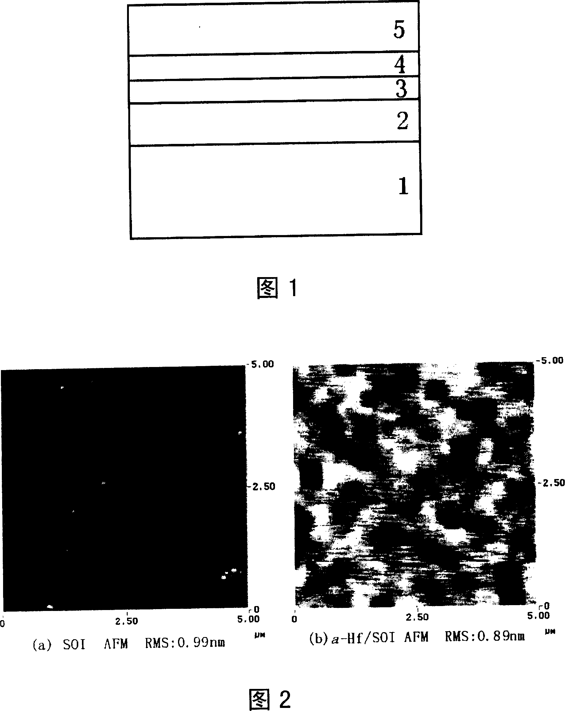
[0043] (1) A conventional SOI covariable substrate is selected for the preparation of an SOI type composite covariable layer substrate. Figure 1 is a schematic structural diagram of the substrate, and the main technical parameters are shown in Table 1.
[0044] Table 1: Main Technical Parameters of SOI Composite Covariable Layer Substrates
[0045]
SOI
composite
covariant
layer substrate
SOI
covariant
Substrate
the bottom
Supporting substrate
1
Material
Silicon (Si)
thickness
(μm)
300-
500
the crystal
quality
single crystal
middle
uncoupling layer
2
Material
(SiOx)
thickness
(nm)
200-
600
the crystal
quality
amorphous o...
PUM
 Abstract
Description
Claims
Application Information