Carbon nano tube field transmitting electronic source

A carbon nanotube, field emission technology, applied in nanotechnology, nanotechnology, nanostructure manufacturing and other directions, to achieve the effect of tight bonding, high electron emission density and emission current, and good electrical connection

Active Publication Date: 2007-10-10
TSINGHUA UNIV +1
View PDF0 Cites 6 Cited by
  • Summary
  • Abstract
  • Description
  • Claims
  • Application Information

AI Technical Summary

Problems solved by technology

Although the existing carbon nanotube field emission electron source has an excellent field emission geometry and a high field enhancement factor (Enhancement Factor), the work function of the carbon nanotube itself is 4.55 electron volts (eV), only Comparable to the work function of tungsten

Method used


Image

  • Carbon nano tube field transmitting electronic source
  • Carbon nano tube field transmitting electronic source
  • Carbon nano tube field transmitting electronic source

Examples


Embodiment Construction

[0024] The present invention will be further described in detail below in conjunction with the accompanying drawings.

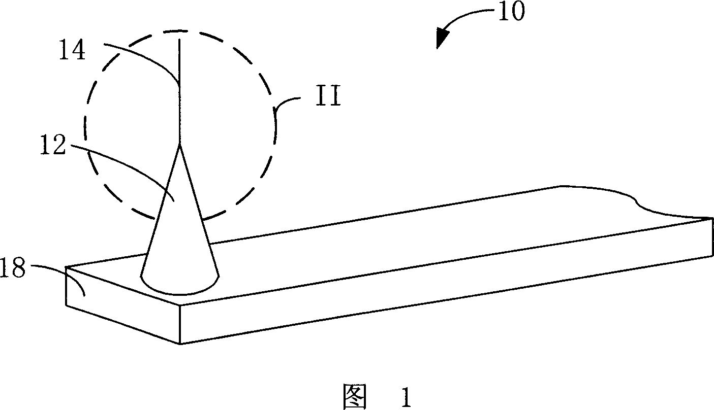
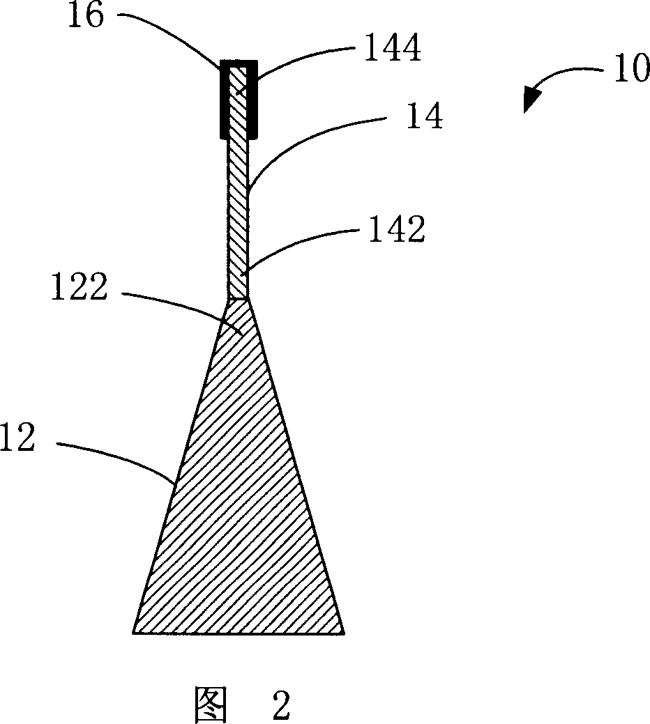
[0025] Please refer to Fig. 1 and Fig. 2, the embodiment of the present invention provides a kind of carbon nanotube field emission electron source 10, this carbon nanotube field emission electron source 10 comprises a conductive substrate 12, a carbon nanotube 14 and a surface modification layer 16 . The conductive base 12 is made of conductive material, such as tungsten, gold, molybdenum, platinum and so on. For the convenience of measurement, the conductive substrate 12 in this embodiment adopts the probe of an atomic force microscope 18 (AtomicForce Microscope, AFM) coated with a gold layer. The conductive base 12 has a top 122 , and the top 122 is tapered. One end 142 of the carbon nanotube 14 is electrically connected to the top 122 of the conductive substrate 12 and adhered to the conductive substrate 12 by van der Waals force. The other end 144 of ...


PUM

PropertyMeasurementUnit
thicknessaaaaaaaaaa
lengthaaaaaaaaaa
diameteraaaaaaaaaa

Abstract

The electron source of field emission of Nano carbon tube includes a current conducting basal body, at least a Nano carbon tube, and a finishing coat. The current conducting basal body possesses a top portion. One end of the Nano carbon tube is connected to the top portion electrically; and the other end is extended out along the top portion. Being distributed and infiltrated on surface of Nano carbon tubes evenly, the finishing coat covers the said extended end. Work function of the finishing coat is lower than work function of the Nano carbon tube.

Description

【Technical field】 [0001] The invention relates to a field emission electron source, in particular to a carbon nanotube field emission electron source. 【Background technique】 [0002] Carbon Nanotube (CNT) is a new type of carbon material, which was discovered by Japanese researcher Iijima in 1991, please refer to "Helical Microtubules of Graphitic Carbon", S.Iijima, Nature, vol.354, p56 (1991) . Carbon nanotubes have excellent electrical conductivity, good chemical stability and large aspect ratio, and they have a tip surface area that is almost close to the theoretical limit (the smaller the tip surface area, the more concentrated its local electric field), so carbon nanotubes in the field The field of emitting vacuum electron sources has potential application prospects. Current studies have shown that carbon nanotubes are one of the best known field emission materials. Its tip size is only a few nanometers to tens of nanometers, has an extremely low field emission voltag...

Claims


Application Information

Patent Timeline
Patent Type & Authority Applications(China)
IPC IPC(8): H01J37/06C01B31/00B82B1/00
CPCH01J9/025B82Y10/00H01J1/3044H01J2201/30469H01J2329/00
Inventor 魏巍姜开利范守善
Owner TSINGHUA UNIV
Why Eureka
Try Eureka