Silicon solar battery

A silicon solar cell and cell technology, applied in the field of solar cells, can solve the problems of high purity requirements, high cost, and low purity of silicon materials, and achieve high photoelectric conversion efficiency, increase light absorption coefficient, and increase junction area.

Inactive Publication Date: 2007-10-17
SHANGHAI SOLAR ENERGY S&T
View PDF0 Cites 5 Cited by
  • Summary
  • Abstract
  • Description
  • Claims
  • Application Information

AI Technical Summary

Problems solved by technology

[0008] In order to solve the problems that the existing silicon solar cell manufacturing technology has too high requirements on the purity of silicon materials, resulting in high costs, and the consumption of a large amount of electric energy and chemical raw materials in the process of prepar

Method used


Image

  • Silicon solar battery
  • Silicon solar battery
  • Silicon solar battery

Examples


Embodiment Construction

[0019] In order to illustrate the practicability of the silicon solar cell structure of the present invention, the present invention will be further described in detail below with reference to the accompanying drawings and a specific embodiment.

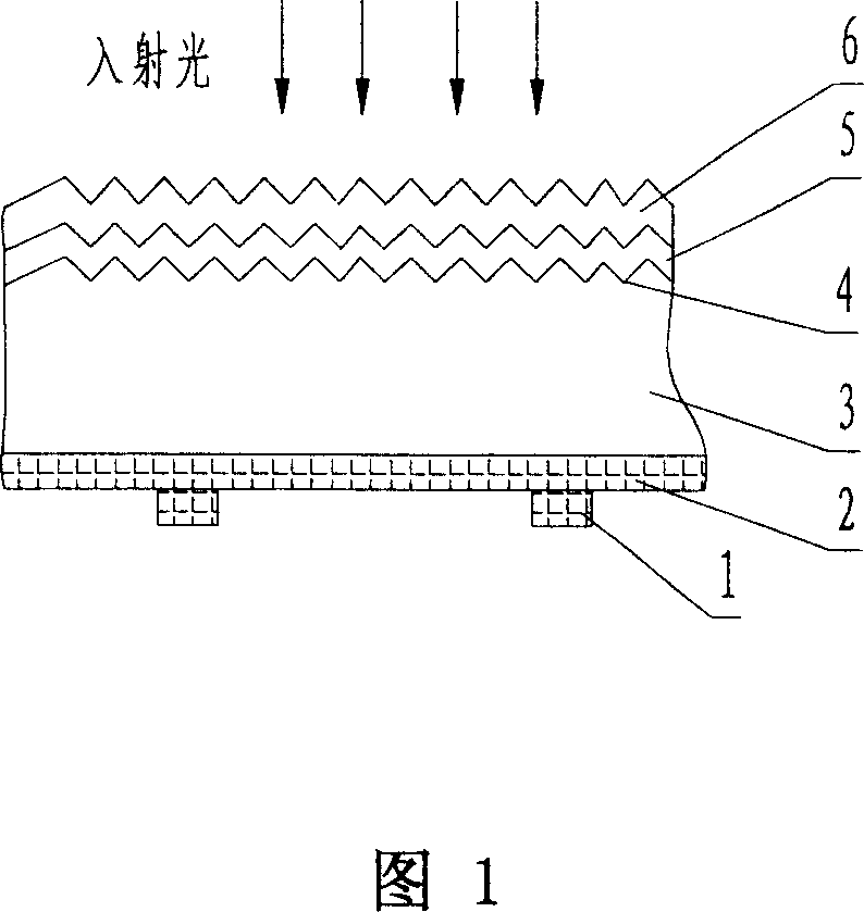
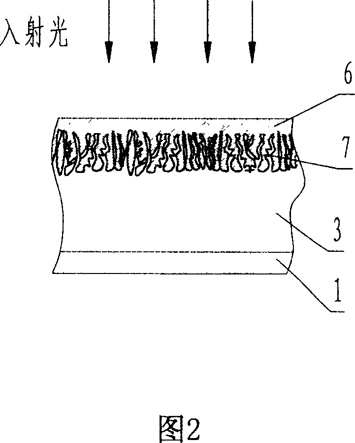
[0020] Fig. 1 is a prior art closest to the present invention, a schematic structural view of a crystalline silicon solar cell with an S1S (semiconductor-dielectric passivation layer-semiconductor) structure. As shown in Figure 1, it includes battery back electrode 1, battery back surface heavily doped layer 2, P-type or N-type semiconductor silicon substrate layer 3, and textured structure on the surface of semiconductor silicon substrate layer material that are sequentially stacked and combined. 4. Dielectric passivation layer 5 and semiconductor thin film layer 6. The above prior art uses the semiconductor SnO 2 A semiconductor heterojunction is formed with the semiconductor silicon substrate layer 3, wherein the dielectric passi...


PUM

PropertyMeasurementUnit
Thicknessaaaaaaaaaa
Sizeaaaaaaaaaa
Thicknessaaaaaaaaaa

Abstract

The invention discloses a silicon solar cell structure, including a battery back electrode, a semiconductor silicon substrate and a semiconductor film layer having Fermi energy level different from the semiconductor silicon substrate. A quasi one-dimensional nanocrystalline body structure is prepared at the surface of material light-receiving surface in the semiconductor silicon substrate. The hole of this nanocrystalline body structure layer is filled by the semiconductor film layer, both of which form a heterojunction having the action of separating the photon-generated carrier. Because of the use of the quantum size effect, the volume effect and the surface effect in the structure, the silicon material with lower purity is used to make the silicon solar cell, and a satisfactory photoelectric conversion efficiency is obtained.

Description

technical field [0001] The invention relates to a solar cell, especially a silicon solar cell that can be manufactured using low-purity crystalline silicon. Background technique [0002] A solar cell is a type of photovoltaic device that directly converts light energy into electrical energy. At present, such devices are mainly made of semiconductor materials. Using the PN junction of semiconductor materials or other structures that can generate self-built electric fields in semiconductor materials, the carriers excited by incident light are separated, and current is generated in the loop through an external circuit. In order to ensure that the carriers excited by the incident light will not be annihilated due to recombination before being separated by the self-built electric field, semiconductor materials are usually required to have extremely high purity. Currently, known silicon solar cells are the most widely used semiconductor silicon material, and its purity is requir...

Claims


Application Information

Patent Timeline
IPC IPC(8): H01L31/042H01L31/0352H01L31/074
CPCY02E10/50
Inventor 李涛勇袁晓
Owner SHANGHAI SOLAR ENERGY S&T
Why Eureka
Try Eureka