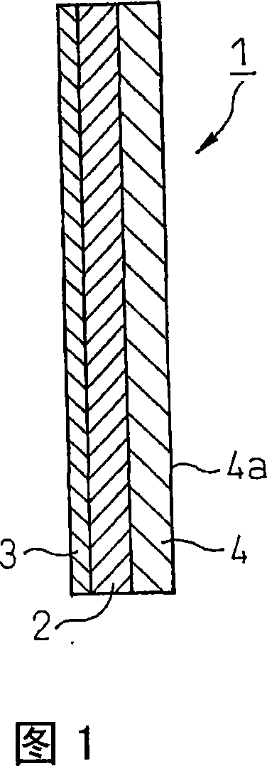
Optical filter

A technology of optical filter and shielding layer, applied in the field of optical filter and its manufacturing, can solve the problems such as the adverse effect of display image tone, and achieve the effect of easy manufacturing and handling, and excellent ease of use

Inactive Publication Date: 2007-10-24
SUMITOMO OSAKA CEMENT CO LTD
View PDF1 Cites 12 Cited by
  • Summary
  • Abstract
  • Description
  • Claims
  • Application Information

AI Technical Summary

Problems solved by technology

However, in the above-mentioned plasma display device, as described in Japanese Unexamined Patent Publication No. 10-319859 (Patent Document 1), since a PDP device including a light-emitting mechanism is provided with a certain space apart from it, There is a filter mechanism composed of a laminated film laminated with several layers of film on the glass, so it cannot be said that it has achieved sufficient weight reduction. In fact, because it is hung on the wall of a general family room , so it is important for the walls to be strong enough, so there will be cases where it is necessary to pre-reinforce the walls themselves
In addition, there are also disadvantages such as double reflection of external light on the display surface due to the reflection of the front glass part of the PDP and the surface and back of the filter.
Since the main form of the electromagnetic wave shielding film generally used in optical filters is etched metal (copper) mesh, or the metal (copper) is exposed on the etched end face, the unique reflection color of metal (copper) Can adversely affect the color tone of the displayed image

Method used


Image

  • Optical filter
  • Optical filter
  • Optical filter

Examples


Embodiment 1

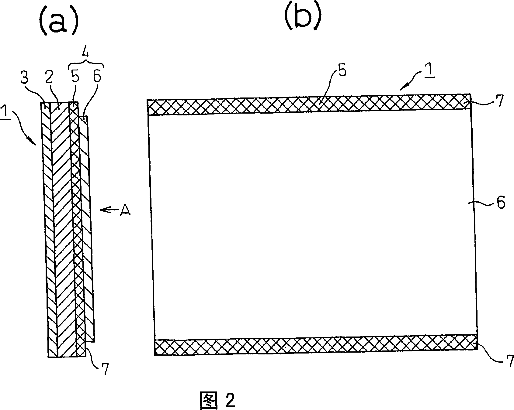
[0159] A 100-μm-thick PET film containing a UV absorber is used as a transparent substrate, and a UV-curable resin layer containing 50% by weight of a silica filler is formed on one side of the film to a thickness of about 1 μm to form a hard coat layer. On it, a conductive medium refractive index layer consisting of a silicon oxide layer containing 85% by weight of antimony-containing tin oxide and having a thickness of about 140 nm is formed, and a silicon oxide layer containing 65% by weight of titanium oxide is formed thereon and A high-refractive-index layer with a thickness of about 110 nm was formed on which a low-refractive-index layer consisting only of silicon oxide and having a thickness of about 90 nm was formed to form an antireflection layer, and a protective film made of PET was laminated on its surface. Then, on the opposite side of the PET film, a paste containing palladium colloid was printed using a screen with a grid-like (mesh) pattern of L / S=30 / 270 (μm), a...

Embodiment 2

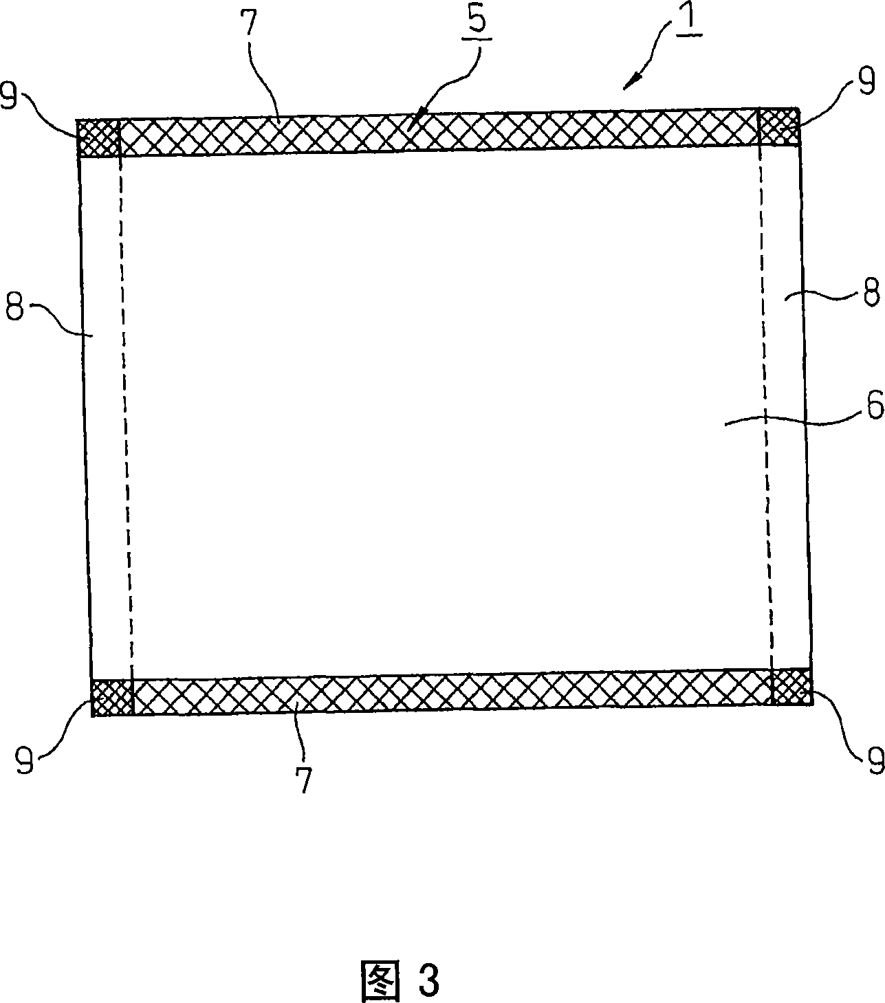
[0167] A PET film containing an ultraviolet absorber with a thickness of 100 μm was used as a transparent substrate, and a hard coat layer, a conductive middle refractive index layer, a high refractive index layer, and a low refractive index layer were formed on one side thereof in the same manner as in Example 1. The anti-reflective layer is laminated with a PET protective film on the surface. Then, on the opposite side of the PET film, a paste containing palladium colloid was printed using a screen with a grid-like (mesh) pattern of L / S=30 / 270 (μm), and it was impregnated in electroless copper In the plating solution, electroless copper plating was performed, followed by electrolytic copper plating, and then Ni-Sn alloy electroplating was performed to form a mesh-shaped electromagnetic wave shielding layer. Then, on the surface of the electromagnetic wave shielding layer, utilize the screen printing method to print the following ink, which contains the following chemical for...

Embodiment 3

[0174] As a transparent base material, a PET film with a thickness of 100 μm containing an ultraviolet absorber was used, and a hard coat layer, a conductive middle refractive index layer, a high refractive index layer, and a low refractive index layer were formed on one side thereof in the same manner as in Example 1. The anti-reflection layer is composed of a protective film made of PET laminated on the surface. Then, on the opposite side of the PET film, a paste containing palladium colloid was printed using a screen with a grid-like (mesh) pattern of L / S=30 / 270 (μm), and it was impregnated in electroless copper In the plating solution, electroless copper plating is carried out, followed by electrolytic copper plating, and then Ni-Sn alloy electroplating is carried out to form a mesh electromagnetic wave shielding layer. Then, on the surface of the electromagnetic wave shielding layer, utilize the screen printing method to print the following ink, which contains the followi...


PUM

PropertyMeasurementUnit
thicknessaaaaaaaaaa
particle sizeaaaaaaaaaa
thicknessaaaaaaaaaa

Abstract

Disclosed is an integrated film-like optical filter wherein an antireflective layer is formed on one side of a transparent base (such as a PET film), a composite layer including an electromagnetic shielding layer and a near-infrared blocking layer is bonded to the other side of the transparent base, and the exposed surface of the composite layer has adhesive properties. This optical filter is light in weight and is easy to produce and handle. In addition, the optical filter is excellent in in-use durability and visibility of visible images, and is useful as an optical filter for display surfaces of plasma displays or the like.

Description

technical field [0001] The present invention relates to an optical filter and its manufacturing method. More specifically, the present invention relates to an optical filter that is laminated and integrated in the form of a film and a method for manufacturing the same, which is used, for example, on a display surface of an optical image display device such as a plasma display. Background technique [0002] Plasma display device (hereinafter sometimes abbreviated as PDP) is made by combining the front glass substrate with display electrodes, bus electrodes, dielectric layer and protective layer; A rear glass substrate having a phosphor layer is bonded so that the electrodes are perpendicular to each other to form a small chamber, and a discharge gas such as xenon gas is sealed in the small chamber. The plasma display device emits light by applying a voltage between the data electrode and the display electrode to cause the discharge of xenon gas. When the xenon gas ions in th...

Claims


Application Information

Patent Timeline
Patent Type & Authority Applications(China)
IPC IPC(8): G02B5/20G02B1/10G02B1/11G02B5/22G09F9/00H05K9/00
Inventor 饭岛智彦石川真章和气正知
Owner SUMITOMO OSAKA CEMENT CO LTD
Why Eureka
Try Eureka