
Arrangement used for manufacturing large area micro-nano structure

A micro-nano structure and large-area technology, which is applied in the direction of photolithography, optics, and opto-mechanical equipment on the pattern surface, can solve the problems of difficulty in making nano-imprint templates, unsuitability for large-area structures, and inability to mass-produce. , to achieve the effects of low development cost, simple optical path adjustment, and simple structure

Inactive Publication Date: 2007-10-31
INST OF OPTICS & ELECTRONICS - CHINESE ACAD OF SCI
View PDF0 Cites 5 Cited by
  • Summary
  • Abstract
  • Description
  • Claims
  • Application Information

AI Technical Summary

Problems solved by technology

Electron beam lithography and ion beam lithography, although high in resolution, are inefficient and not suitable for fabricating large-area structures
Although nanoimprint technology has the advantages of high resolution and good repeatability, it encounters great difficulties in the production of large-area nanoimprint templates.
The existing micro-nano processing technology has a series of problems such as high cost, low efficiency, and incapability of large-scale production. The production of large-area micro-nano structures encounters severe challenges. It is urgent to develop other types of low-cost equipment to meet the needs of nano-compounds. Requirements for large-area micro-nano structure fabrication technology in the fields of semiconductor circuits, nano-MEMS, integrated optics, and magnetic information storage

Method used


Image

  • Arrangement used for manufacturing large area micro-nano structure
  • Arrangement used for manufacturing large area micro-nano structure
  • Arrangement used for manufacturing large area micro-nano structure

Examples


Embodiment Construction

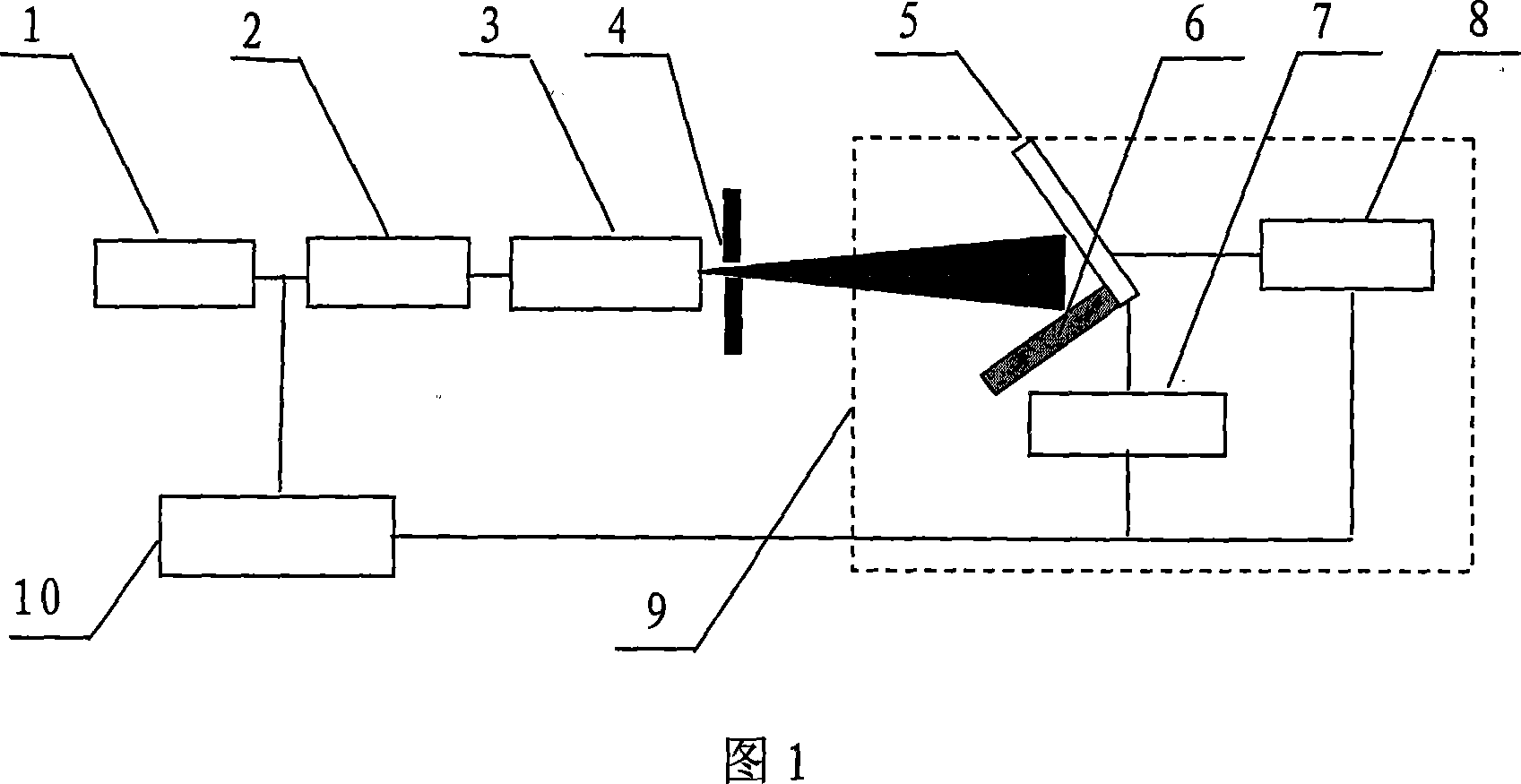
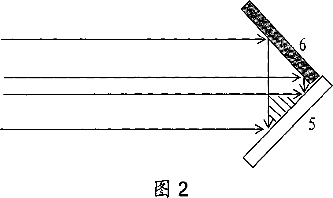
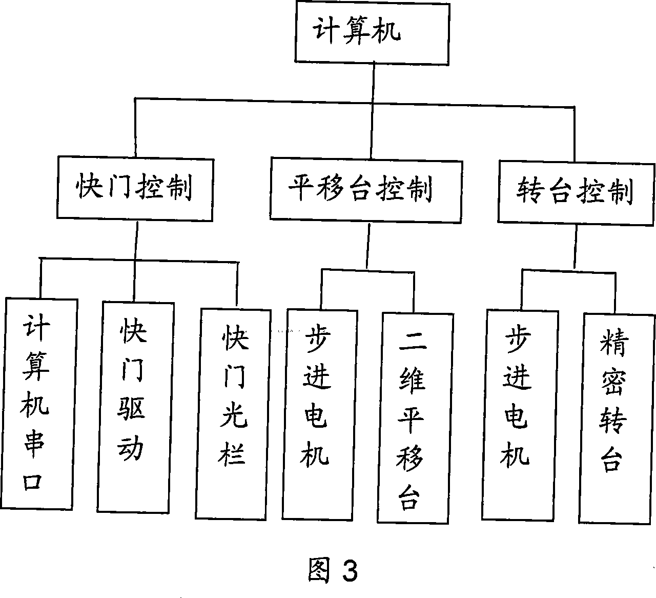
[0017] As shown in Figure 1, the present invention mainly comprises a coherent light source 1, a shutter 2, a spatial filter 3, an aperture 4, a sample stage 5, a mirror 6, a precision turntable 7, a two-dimensional translation stage 8, a local darkroom 9, and a computer. control system 10. The laser beam is emitted by a coherent light source 1, and enters the spatial filter 3 through the shutter 2 and mirror 6. After the spatial filter 3 improves the spatial coherence and beam uniformity, the stray light and the size of the beam are controlled by the diaphragm 4, and finally irradiated On mirror 6 and sample stage 5. The sample stage 5 is fixed on the two-dimensional translation stage 7 at first, and then it is vertically fixed on the precision turntable 7 together with the mirror 6 . The opening and closing of the shutter 2 , the movement of the two-dimensional translation platform 8 and the rotation of the precision turntable 7 are completed by the computer control system ...


PUM


Abstract

This invention relates to one large area nanometer structure process device, which mainly comprises the following parts: coherent source, shot, space filter, light grating, sample bench, reflection lens, fine rotation bench, two dimensional mobile bench, local dark chamber and computer control system, wherein the sample bench, reflection lens, fine rotation bench and two dimensional bench are put into local dark chamber; the laser beam is sent from coherent source through shot into space filter to improve the beam even property and then through light grating size and finally onto reflection lens and sample bench; shot is switched and two dimensional mobile bench and fine rotation bench are fulfilled by computer control system.

Description

technical field [0001] The invention relates to a device for making large-area micro-nano structures. Background technique [0002] At present, the technologies used to fabricate micro-nano structures mainly include: optical lithography, electron beam lithography, ion beam lithography, and nanoimprint technology. However, when producing large-area micro-nano structures, for optical lithography, the exposure wavelength of the lithography system is getting shorter and shorter, the numerical aperture of the system is getting bigger and bigger, and the contradiction between resolution and depth of focus is getting more and more prominent. Electron beam lithography and ion beam lithography, although high in resolution, are inefficient and unsuitable for fabricating large-area structures. Although nanoimprint technology has the advantages of high resolution and good repeatability, it encounters great difficulties in the fabrication of large-area nanoimprint templates. The existi...

Claims


Application Information

Patent Timeline
Patent Type & Authority Applications(China)
IPC IPC(8): G03F7/00
Inventor 陈献忠罗先刚张春梅姚汉民杜春雷李海颖
Owner INST OF OPTICS & ELECTRONICS - CHINESE ACAD OF SCI
Learn More