High-purity implanting planar array microelectrode and its production

A planar array and manufacturing method technology, applied in the direction of electrodes, artificial respiration, physical therapy, etc., can solve the problems of increasing the density of micro-electrode arrays, complex manufacturing process, and difficult realization, so as to improve the stimulation or recording effect, simple manufacturing process, Ease of mass production

Inactive Publication Date: 2007-11-21
SHANGHAI INST OF MICROSYSTEM & INFORMATION TECH CHINESE ACAD OF SCI
View PDF0 Cites 17 Cited by
  • Summary
  • Abstract
  • Description
  • Claims
  • Application Information

AI Technical Summary

Problems solved by technology

However, the existing problem is that when making a high-density microelectrode array, the electrode area will increase exponentially. On the basis of maintaining the original electrode area, increasing the density of the micro-electrode array, the wiring problem becomes a difficult point
Someone proposed to control the electrodes by making organic field effect transistors (organic field effect transistors) and adopting the method of matrix addressing, so that the micro-electrode matrix with M×N distribution can be controlled only by M+N wires instead of M×N wires [Dara Feili, et al. "Flexible organic field effect transistors for biomedical microimplants using polyimide and parylene C as substrate and insulator layers", J.Micromech.Microeng., 2006, 16: 1555-1561], although this method reduces the number, but the production process is complicated and it is difficult to realize

Method used


Image

  • High-purity implanting planar array microelectrode and its production
  • High-purity implanting planar array microelectrode and its production
  • High-purity implanting planar array microelectrode and its production

Examples


Embodiment 1

[0018] The specific characteristics of the high-density implantable planar array microelectrode manufacturing method provided by the present invention are further described below in conjunction with the accompanying drawings:

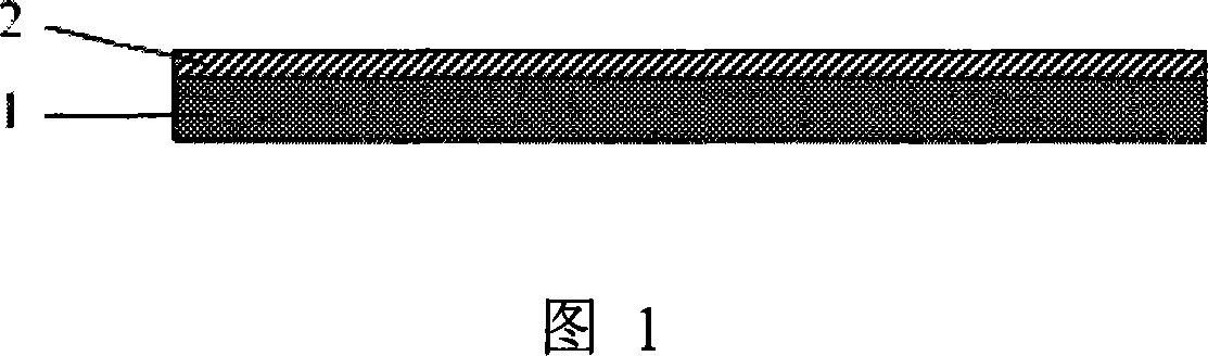
[0019] 1) Clean the silicon wafer 1 with a conventional semiconductor process cleaning method, and prepare an aluminum film 2 with a thickness of about 1 micron on the surface, as a sacrificial layer for electroplating conductive structures and release (Fig. 1);

[0020] 2) Baking the silicon wafer at 120°C for 20 minutes, spin-coating 6809 photoresist (3000 rpm, 30 seconds) on the aluminum film layer of the silicon wafer, and pre-baking at 80°C for 20 minutes;

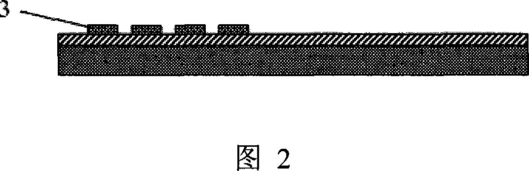
[0021] 3) Photolithography, sputtering Ti / Pt / Ti (2500 Ȧ), combined with Lift-off process, forming electrode stimulation site or recording site metal layer 3 (Fig. 2);

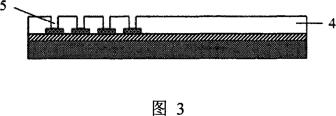
[0022] 4) Spin-coat photosensitive polyimide Durimide 7510 (3000 rpm, 30 seconds), make an isolation insulating layer 4, and f...


PUM


Abstract

The invention is concerned with a kind of high density and implantation plane array microelectrode and its produce method. The said array microelectrode uses polymer as insulated layer material and the leads connects with the electrode activating location or record location of different insulated layers. Produce through hole on the isolation insulated layer and form metal connecting structure in the through hole by plating process to connect the leads with upper and down electrode activating location or record location on the isolation insulated layer. Polishing the upper surface with chemistry polishing after the plating process in order that can keep the well connecting between plating metal pole and upper layer spattering metal layer. This produce method can produce higher density array micro electrode on unit area than the one of common lead setting on single layer to realize the activation or record with higher selectivity to implantation array micro electrode.

Description

technical field [0001] The invention relates to a method for manufacturing a high-density implanted planar array microelectrode, which can be applied to the fields of neurological disease treatment, neurobiological basic research and the like, and belongs to the field of implanted microelectrodes. Background technique [0002] Neural engineering system is currently a very active and rapidly developing research field, such as brain-computer interface, neural prosthesis and other issues have received more and more attention. In a neuroengineered system, the most fundamental and critical part is the neuro-electronic interface, the electrodes. According to different objects of action and application goals, people have successively researched and developed various forms of implantable microelectrodes, including hoop-shaped microelectrodes, needle-shaped array microelectrodes, planar array microelectrodes, and sieve-shaped microelectrodes. Among them, the planar array microelectr...

Claims


Application Information

Patent Timeline
Patent Type & Authority Applications(China)
IPC IPC(8): A61N1/04A61N1/36
Inventor 李刚孙晓娜周洪波姚源赵建龙
Owner SHANGHAI INST OF MICROSYSTEM & INFORMATION TECH CHINESE ACAD OF SCI
Why Eureka
Try Eureka