Organic ultraviolet optical sensor based on phosphorescence material light diode

A photovoltaic diode and organic ultraviolet light technology, which is applied in the field of organic ultraviolet light optical sensors, can solve problems such as high cost, low response sensitivity, and complicated preparation process, and achieve the effects of light weight, high sensitivity, and small volume

Inactive Publication Date: 2008-01-09
CHANGCHUN INST OF OPTICS FINE MECHANICS & PHYSICS CHINESE ACAD OF SCI
View PDF0 Cites 9 Cited by
  • Summary
  • Abstract
  • Description
  • Claims
  • Application Information

AI Technical Summary

Problems solved by technology

[0003] Aiming at the problems of complex preparation process and high cost of using inorganic ultraviolet light sensitive devices as optical sensors in the prior art, and the spectral response of organic/polymer photovoltaic diodes mostly covers the visible region, and fluorescent materials are used, and fluorescent materials As a problem that the response sensitivity of ultraviolet light sensitive devices to ultraviolet light becomes low, the present invention provides an organic ultraviolet light optical sensor based

Method used


Image

  • Organic ultraviolet optical sensor based on phosphorescence material light diode

Examples


Embodiment 1

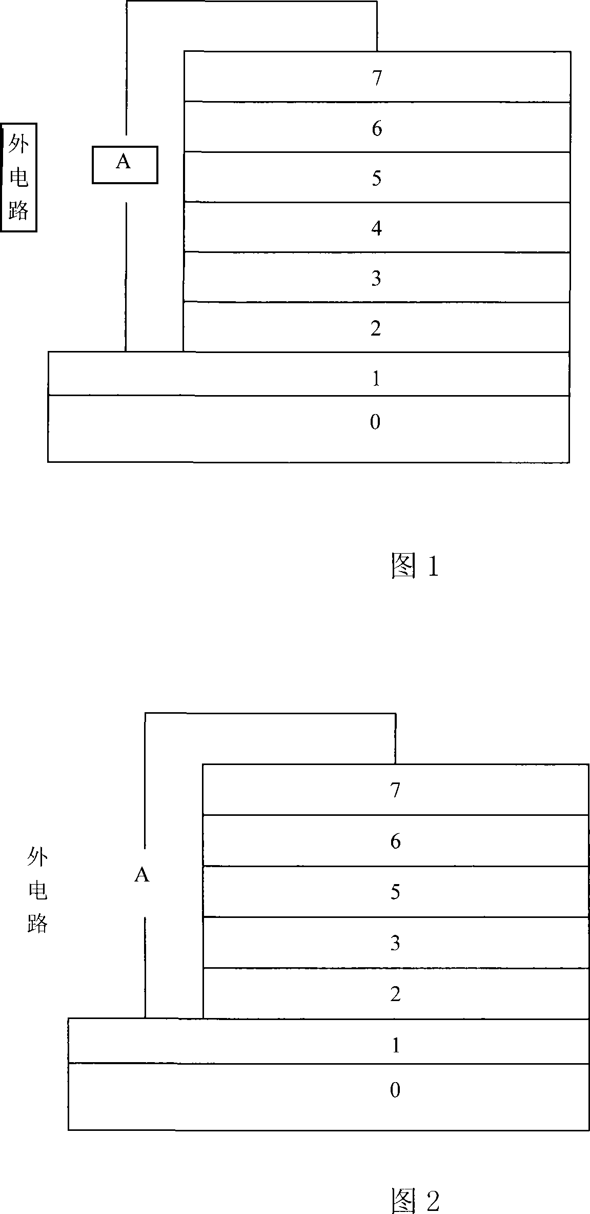
[0024] The device structure shown in FIG. 1 is selected: in this embodiment, firstly, the hole-collecting electrode layer 2 selects the ITO film on the glass substrate 1 as the transparent conductive film. After cleaning the transparent conductive film on the substrate 1, at first in high vacuum (3-2x10 -1 Pascal), on the transparent conductive film, deposit one deck thickness and be 10nm electron donor layer 3, the material of electron donor layer 3 adopts TPD; Then on the electron donor layer 3, deposit the mixed layer of electron donor and electron acceptor 4. The thickness is 5nm, the electron donor material is TPD, and the electron acceptor material is Ir(ppy) 3 , TPD and Ir(ppy) 3 The weight ratio of the electron acceptor layer 5 is 1: 1; the electron acceptor layer 5 is deposited on the mixed layer 4 of the electron donor and the electron acceptor, and the material of the electron acceptor layer 5 is Ir (ppy) 3 , the thickness is selected as 20nm or 30nm or 40nm; afte...

Embodiment 2

[0026] The hole collecting electrode layer 2 selects the ITO film on the glass substrate 1 as a transparent conductive film, and the electron donor layer 3 selects m-MTDATA material with a thickness of 6nm; The mixed layer 4 of the acceptor has a thickness of 5nm, the material of the electron donor is m-MTDATA, and the material of the electron acceptor is Btp 2 Ir(acac), m-MTDATA and Btp 2 The weight ratio of Ir (acac) is 1: 1; Then deposit electron acceptor layer 5 on the mixed layer 4 of electron donor and electron acceptor, electron acceptor layer 5 selects material as Btp 2Ir (acac), the thickness is selected as 20nm or 30nm or 35nm; after that, an electron collection layer 6 is deposited on the electron acceptor layer 5, and the material of the electron collection layer 6 is LiF, and its thickness is 0.8nm; finally on the electron collection layer 6 The electron collecting electrode layer 7 is deposited, and the electron collecting electrode layer 7 is made of metal Al m...

Embodiment 3

[0029] The hole collecting electrode layer 2 selects the ITO film on the glass substrate 1 as a transparent conductive film; the electron donor layer 3 selects m-MTDATA material with a thickness of 15nm; the thickness of the mixed layer 4 of the electron donor and electron acceptor is 5nm, The electron donor material is m-MTDATA, and the electron acceptor is Ir(ppy) 3 , m-MTDATA and Ir(ppy) 3 The weight ratio is 1:1,; electron acceptor layer 5 selects Ir (ppy) 3 , the thickness is selected as 20nm or 25nm or 30nm; after that, an electron collection layer 6 is deposited on the electron acceptor layer 5, and the material of the electron collection layer 6 is LiF, and its thickness is 1.5nm; finally, an electron collection electrode is deposited on the electron collection layer 6 Layer 7, the electron collecting electrode layer 7 is made of metal Al, and its thickness is 120nm.

[0030] Adopt the measuring method described in embodiment 1 to measure result as follows:

[0031]...


PUM

PropertyMeasurementUnit
Thicknessaaaaaaaaaa
Thicknessaaaaaaaaaa
Thicknessaaaaaaaaaa

Abstract

The invention is concerned with the organic ultraviolet rays (UV) optical transducer bases on the phosphorescence material, belongs to the UV sensitivity optical transducer technique field, which applies the existed compound that is with the low ionized power (IP) and upper hole transmission specialty as the donor, and applies the phosphorescence compound that is with the high electron affinity (EA) and the bigger electron transmission specialty as the acceptor, to extend the choice of material availability; the device, with the simple making method of applying the multi-medium structure and the method of heat evaporation for filming with low cost; and so, having the device in small volume, low weight by applying the thin organic medium and the metal electrode layer; and because of the longer excited state life cycle , the exaction diffusion length of the phosphorescence, it is with higher efficiency than the organic polymer photovoltaic diode of the fluorescence material, not only represents on higher response sensitivity against the UV, just to the 300-400nm wave band UV and treats the visible light as the blind zone. The invention is available to use in the science, the industrial, and the commercial fields.

Description

technical field [0001] The invention belongs to the technical field of ultraviolet light-sensitive optical sensors, and relates to an organic ultraviolet light optical sensor based on phosphorescent material organic diodes. Background technique [0002] The photon-electron conversion of organic materials requires the decomposition of excitons generated by optical absorption into charge carriers, and this optical absorption is different from ordinary solar cells. The light absorption spectrum of organic solar cells is required to mainly cover the visible region (400-700nm). The ultraviolet light irradiated by sunlight on the ground is mainly in the 300-400nm band, and the light irradiated on the ground is mainly in the visible light band, while the ultraviolet optical sensor is required to be sensitive to a small amount of ultraviolet light in the band (300-400nm). At present, ultraviolet light optical sensors mainly use inorganic ultraviolet light sensitive devices as optica...

Claims


Application Information

Patent Timeline
IPC IPC(8): H01L51/42
CPCY02E10/50Y02E10/549
Inventor 李文连孔治国车广波初蓓毕德锋
Owner CHANGCHUN INST OF OPTICS FINE MECHANICS & PHYSICS CHINESE ACAD OF SCI
Why Eureka
Try Eureka