

Method of forming metallic pattern, metallic pattern and printed wiring board using it and tft wiring circuit
A technology of metal graphics and graphic forms, which is applied in the direction of printed circuit, printed circuit manufacturing, metal material coating process, etc., can solve the problems of conductivity limitation, etc., and achieve the effect of high precision and high adhesion
- Summary
- Abstract
- Description
- Claims
- Application Information
AI Technical Summary
Problems solved by technology
Method used
Image

Examples
Embodiment (2
[0148] In the embodiment (2), the graft pattern is formed by bringing a compound having a polymerizable group and a functional group reactive with the electroless plating catalyst or its precursor into contact with the substrate and then patternwise irradiating radiation rays. In the following description, a "functional group that reacts with an electroless plating catalyst or its precursor" may be referred to as an "interactive group", and a compound having a polymerizable group and an interactive group is referred to as a "containing polymerizable Reciprocal Groups of Composition".
[0149] Grafting patterns by surface grafting
[0150] In the embodiment (2), by bringing the polymerizable compound containing the mutual reactive group into contact with the substrate and applying energy in the form of patterns, it is possible to create a gap between the polymerizable group of the polymerizable compound containing the reactive group and the substrate. A chemical bond is formed, ...
Embodiment
[0319] Hereinafter, the present invention will be described in detail with reference to Examples, but it should be understood that the present invention is not limited to these Examples.
[0320] Examples and comparative examples related to the use of a surface charge improver are Examples 1-1 to 1-4 in preparation for substrates.
[0321] The following composition having the following general formula was coated on the surface of a polyimide film (KAPTON®, manufactured by DuPont-Toray) as a raw material by using a coating bar of rod No. 18, and heated at 80° C. Drying was carried out for 2 minutes to provide an intermediate layer having a thickness of 6 μm.
[0322] After thus obtaining the raw material having the intermediate layer, it was precured by light irradiation for 10 minutes using a 400 W high-pressure mercury lamp (trade name: UVL-400P, manufactured by Riko Kagaku Sangyo), so as to prepare the substrate used in Example 1-1 a.
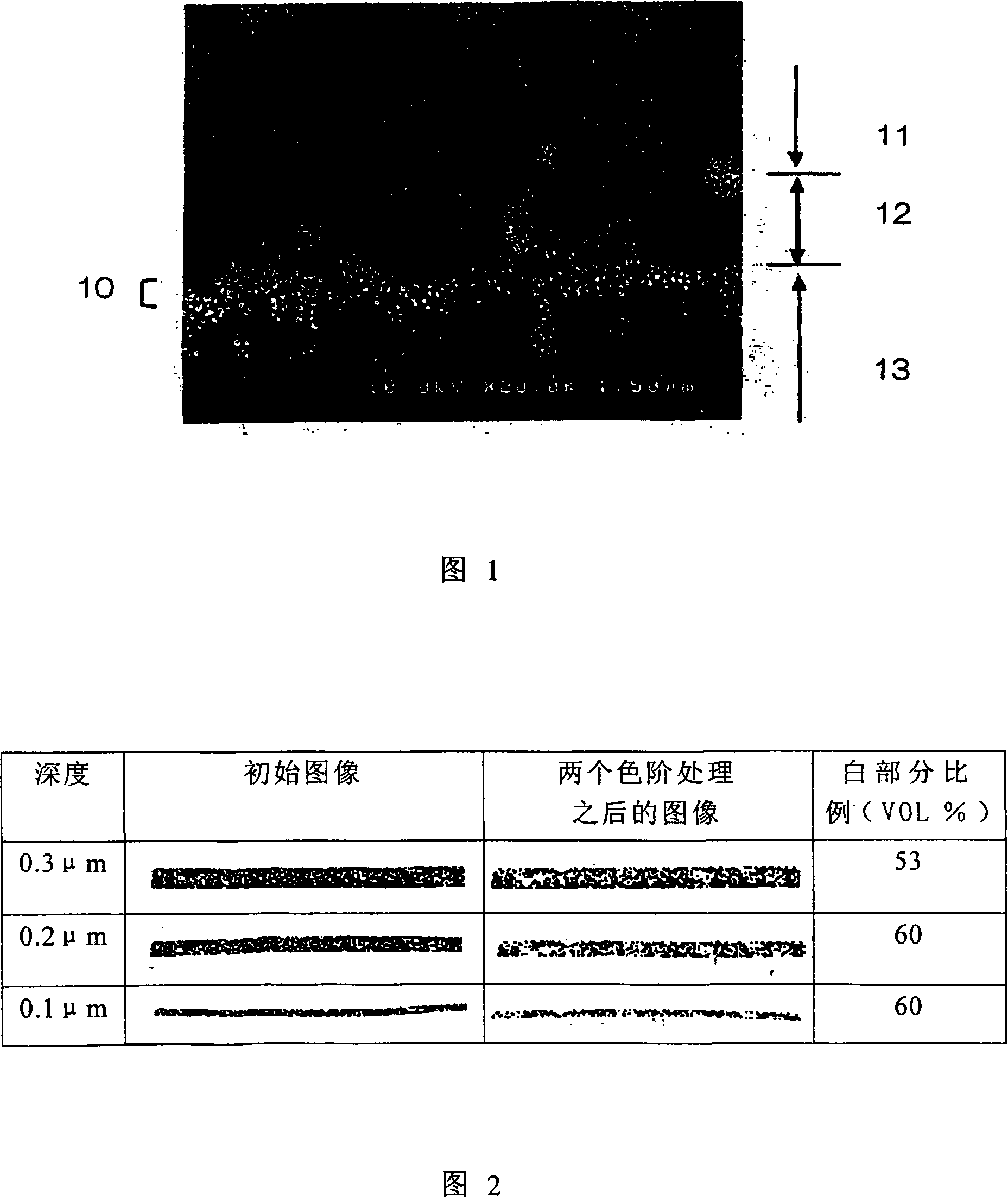
[0323] Rz of the raw material, polyi...
Embodiment 1-5 to 1-8
[0350] Acrylic was applied to the surface of the substrate A prepared in a similar manner to Example 1-1 with a #6 bar, and the coated surface was laminated with a PET film having a thickness of 25 μm.
[0351] Also, after a chrome deposition mask pattern having a pattern of 5 μm line length and 25 μm gap width and a pattern of 10 μm line length and 20 μm gap width were provided thereon, the substrate A was exposed to UV light (400 W high-pressure mercury lamp: UVL-400P, manufactured by Piko Kagaku Sangyo Co., irradiation period: 30 seconds). After light irradiation, the mask and the overlay film were removed, and the substrate was rinsed with water to provide a grafted pattern material 1-B having polyacrylic acid grafted in a patterned form.
[0352] The Rz of the patterned area of the grafted patterning material 1-B determined in a similar manner to that of the polyimide film raw material was 14 nm.
[0353] form metal pattern
[0354] The graft pattern material 1-B was ...
PUM
| Property | Measurement | Unit |
|---|---|---|
| Thickness | aaaaa | aaaaa |
| Thickness | aaaaa | aaaaa |
| Thickness | aaaaa | aaaaa |
Abstract
Description
Claims
Application Information