Universal film material graphics method

A thin-film material, graphic technology, applied in metal material coating process, gaseous chemical plating, process for producing decorative surface effects, etc. High-quality, easy-to-promote, and uncomplicated processes

Inactive Publication Date: 2008-03-19
SHANGHAI JIAO TONG UNIV
View PDF0 Cites 24 Cited by
  • Summary
  • Abstract
  • Description
  • Claims
  • Application Information

AI Technical Summary

Problems solved by technology

This process has the advantages of mass production and precision better than stereolithography, but its patterning is limited to metal or alloy materials that can achieve electrochemical deposition
[0007] In summary, due to the limitations of the existing patterning process, although for some specific materials, an ideal process can be selected through research, there is currently no integrated general patterning method that does not rely on thin film materials. There are not too many restrictions on the thickness, and the graphics quality is high, and graphics with high flatness can be obtained

Method used


Image

  • Universal film material graphics method
  • Universal film material graphics method

Examples


Embodiment 1

[0048] Main material:

[0049] Substrate: 3 mm thick optical glass substrate

[0050] Disposable Planar Micromold Material: Photoresist (AZ4620)

[0051] Film material: polyimide (Beijing Bomi Technology Co., Ltd. ZKPI-305II glue)

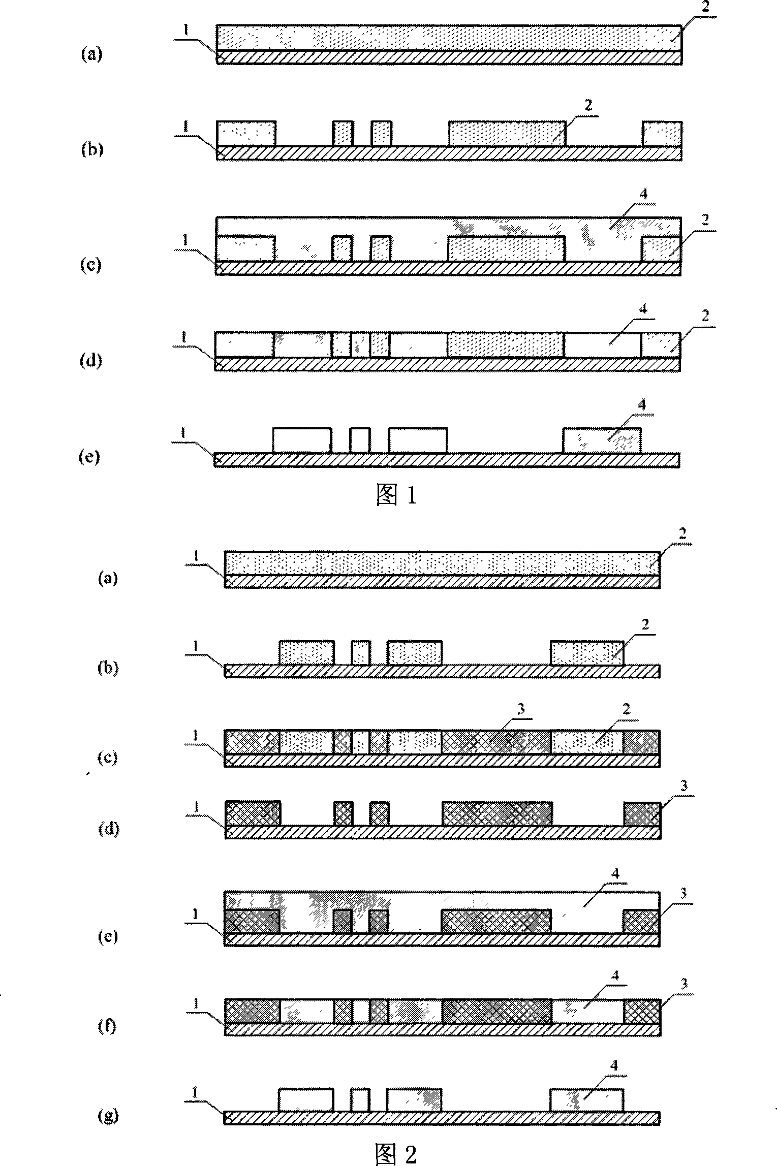
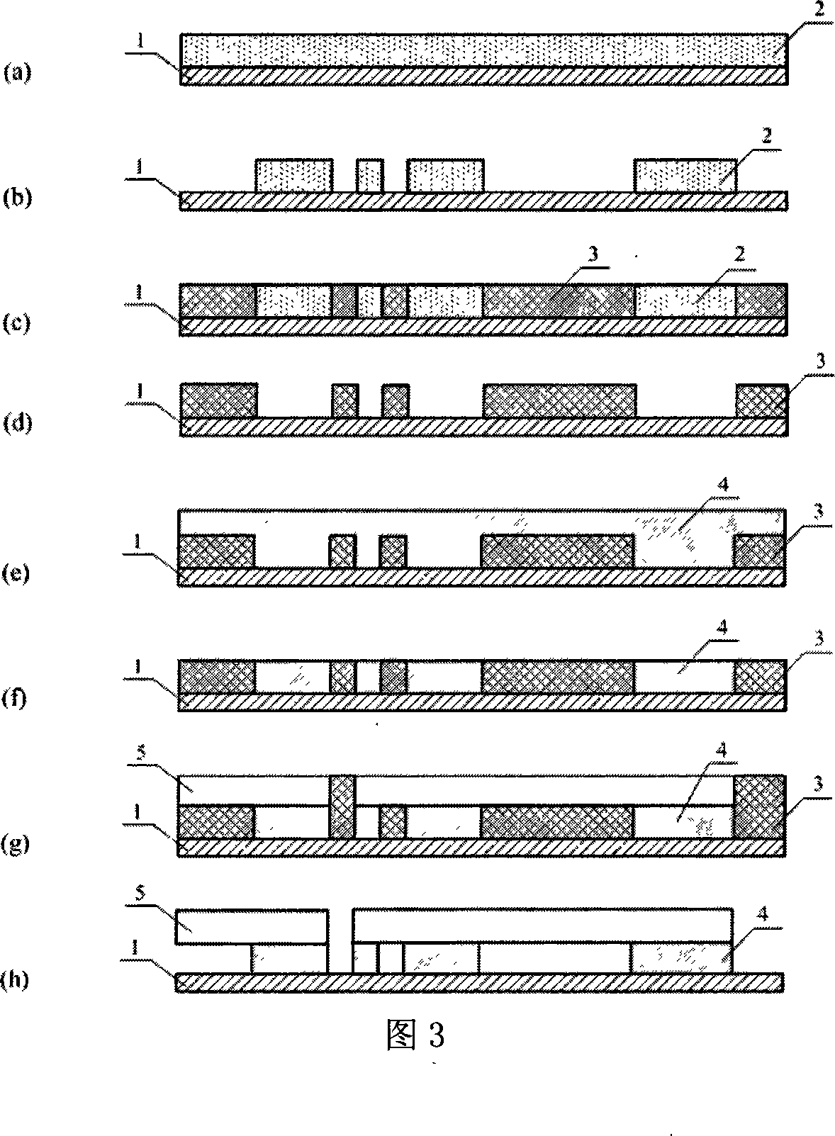
[0052] As shown in Figure 1, the optical glass substrate 1 is first cleaned sequentially with acetone and deionized water. After drying and drying, the AZ4620 photoresist 2 with a thickness of 22 microns is spin-coated, and a disposable planar micro-surface is formed by conventional ultraviolet lithography and development. The pattern of the mold, the gap of the pattern is a rectangular shallow groove array with a length of 60 microns and a width of 20 microns, which is the position of the microstructure of the film to be formed.

[0053] The polyimide film 4 is deposited by spinning to fill up the voids of the micro-mold. After the deposition of the polyimide film is completed, at first grind the surface of the substrate covered by polyimide wi...

Embodiment 2

[0057] Main material:

[0058] Substrate: 3 mm thick optical glass substrate

[0059] Disposable planar micromold material: metallic copper

[0060] Film material: polyimide (Beijing Bomi Technology Co., Ltd. ZKPI-305II glue)

[0061] As shown in FIG. 2 , firstly, the optical glass substrate 1 is cleaned sequentially with acetone and deionized water, and after drying, the Cr / Cu seed layer is sputtered. AZ4620 photoresist 2 is spin-coated with a thickness of 22 microns, and a mask used for electroplating is formed by conventional ultraviolet lithography and development, that is, a photoresist rectangular array with a length of 60 microns and a width of 20 microns (same as the final microstructure pattern made ).

[0062] Use a high-dispersion copper sulfate plating solution to perform mask electroplating on the patterned substrate after photolithography, and grow a 22-micron thick metal copper plating layer 3 on the photolithographically exposed seed layer, flush with the ph...

Embodiment 3

[0069] Main material:

[0070] Substrate: 2 mm thick optical glass substrate

[0071] Disposable planar micromold material: metallic copper

[0072] Film material: polyimide (Beijing Bomi Technology Co., Ltd. ZKPI-305II glue), carbon nanotubes (Shenzhen Nanoport Co., Ltd. SMWNTS-2040)

[0073] As shown in FIG. 2 , firstly, the optical glass substrate 1 is cleaned sequentially with acetone and deionized water, and after drying, the Cr / Cu seed layer is sputtered. AZ4620 photoresist 2 is spin-coated with a thickness of 22 microns, and a mask used for electroplating is formed by conventional ultraviolet lithography and development, that is, a photoresist rectangular array with a length of 60 microns and a width of 20 microns (same as the final microstructure pattern made ).

[0074] Use a high-dispersion copper sulfate plating solution to perform mask electroplating on the patterned substrate after photolithography, and grow a 22-micron thick metal copper plating layer 3 on the...


PUM

PropertyMeasurementUnit
lengthaaaaaaaaaa
widthaaaaaaaaaa
thicknessaaaaaaaaaa

Abstract

The invention discloses a graphic method for a universal film material in the technical field of micro machine processing. The invention prepares a disposable plane micro mould on a basal by photolithograph or mask plating; the film material is deposited on the whole basal, to fill the gap of the micro mould; the redundant part of the film which is higher than the micro mould is removed by grinding, and the film is reduced to be as thick as required; the disposable plane micro mould is removed selectively, to obtain the required micro structure. The invention can manufacture not only manufacture single structures but also laminated structures; can integrate with the sacrificial layer process to manufacture a suspend structure; is not restrained by the material, thickness and deposition method of the film and the substrate material, and is universal; solves the problem that conventional methods of some film materials cannot manufacture quite thick and neat boundary micro structures; has simple process and quite high graphic quality; is compatible with conventional micro processing technologies; does not need special processes and equipments; and is easy to be promoted.

Description

technical field [0001] The invention relates to a method in the technical field of micromachining, in particular to a patterning method for a universal thin film material. Background technique [0002] Micromachining is a means of manufacturing microsensors, microactuators, microstructures and systems, including thin film growth, patterning processes, bonding operations, sacrificial layer processes, etc. The patterning process refers to the process of transferring the pattern of the mask plate to the photoresist and then onto the film through photolithography. It determines the geometric size and flatness of the manufactured microstructure, and is a key technology in micromachining. The step of transferring the pattern of photoresist to the film can be achieved by etching the film first and then photolithography, or by mask plating and selective chemical vapor deposition (CVD) after photolithography and film growth. and stripping technology implementation. However, these t...

Claims


Application Information

Patent Timeline
Patent Type & Authority Applications(China)
IPC IPC(8): B81C1/00
Inventor 丁桂甫蔡豪刚杨卓青
Owner SHANGHAI JIAO TONG UNIV
Why Eureka
Try Eureka