

Emitting surface semiconductor LED with nanostructure and its preparing process
A technology of light-emitting diodes and nanostructures, applied in semiconductor devices, electrical components, circuits, etc., can solve the problems of low repeatability and increased cost, and achieve the effect of being beneficial to mass production, expanding the scope, and increasing the current density
- Summary
- Abstract
- Description
- Claims
- Application Information
AI Technical Summary
Problems solved by technology
Method used
Image

Examples
Embodiment 1
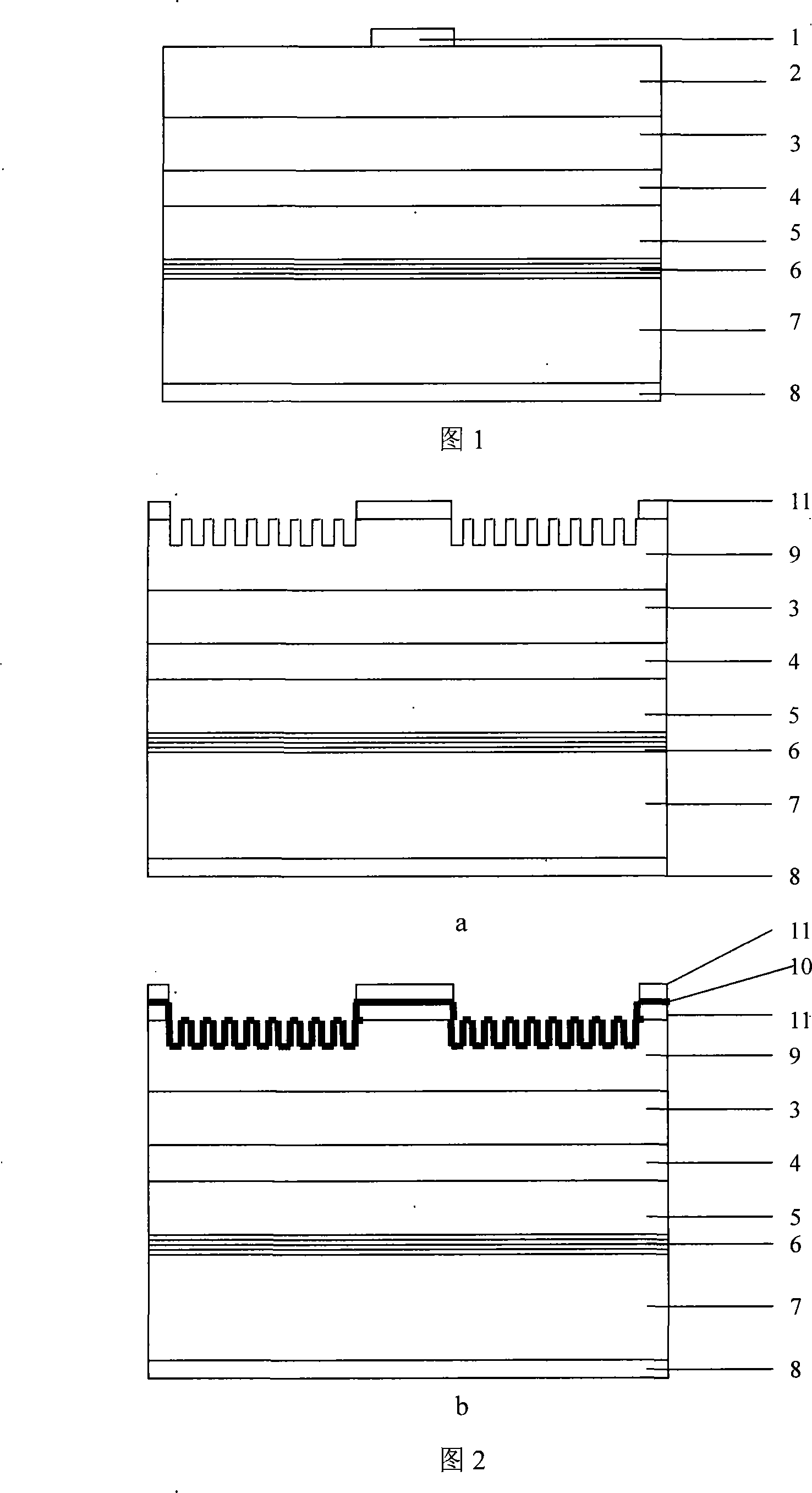
[0042] 1) AlGaAs / AlAs composite Bragg reflective layer DBR 6, N-type lower confinement layer 5, multi-quantum active region 4, and P-type upper confinement layer 3 are sequentially grown on the substrate 7 by metal-organic chemical vapor deposition (MOCVD) equipment for 40 cycles and a GaP layer 2, the thickness of the GaP layer 2 is 8 μm;
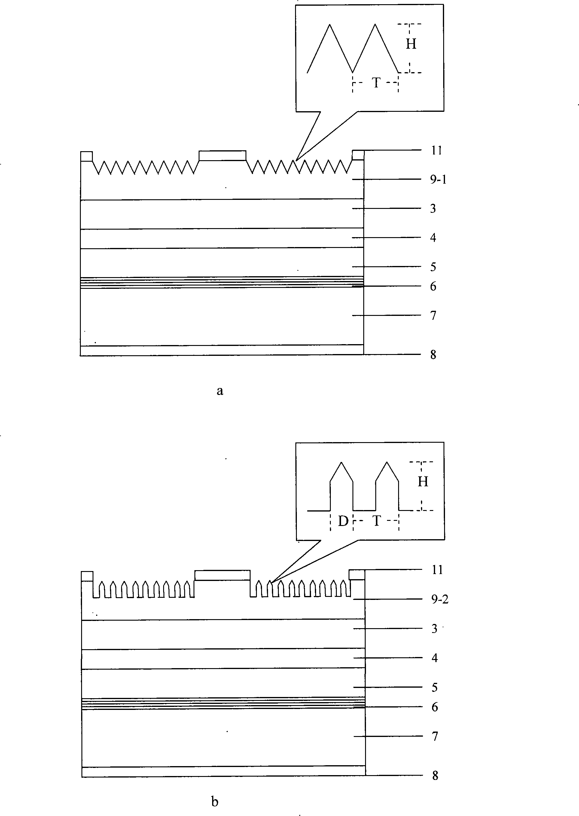
[0043] 2) On the upper surface of the GaP layer 2, a P-type electrode with a grid structure of a metal frame is prepared, the plane figure is shown in Figure 5b, and the electrode size is 300 μm×300 μm;
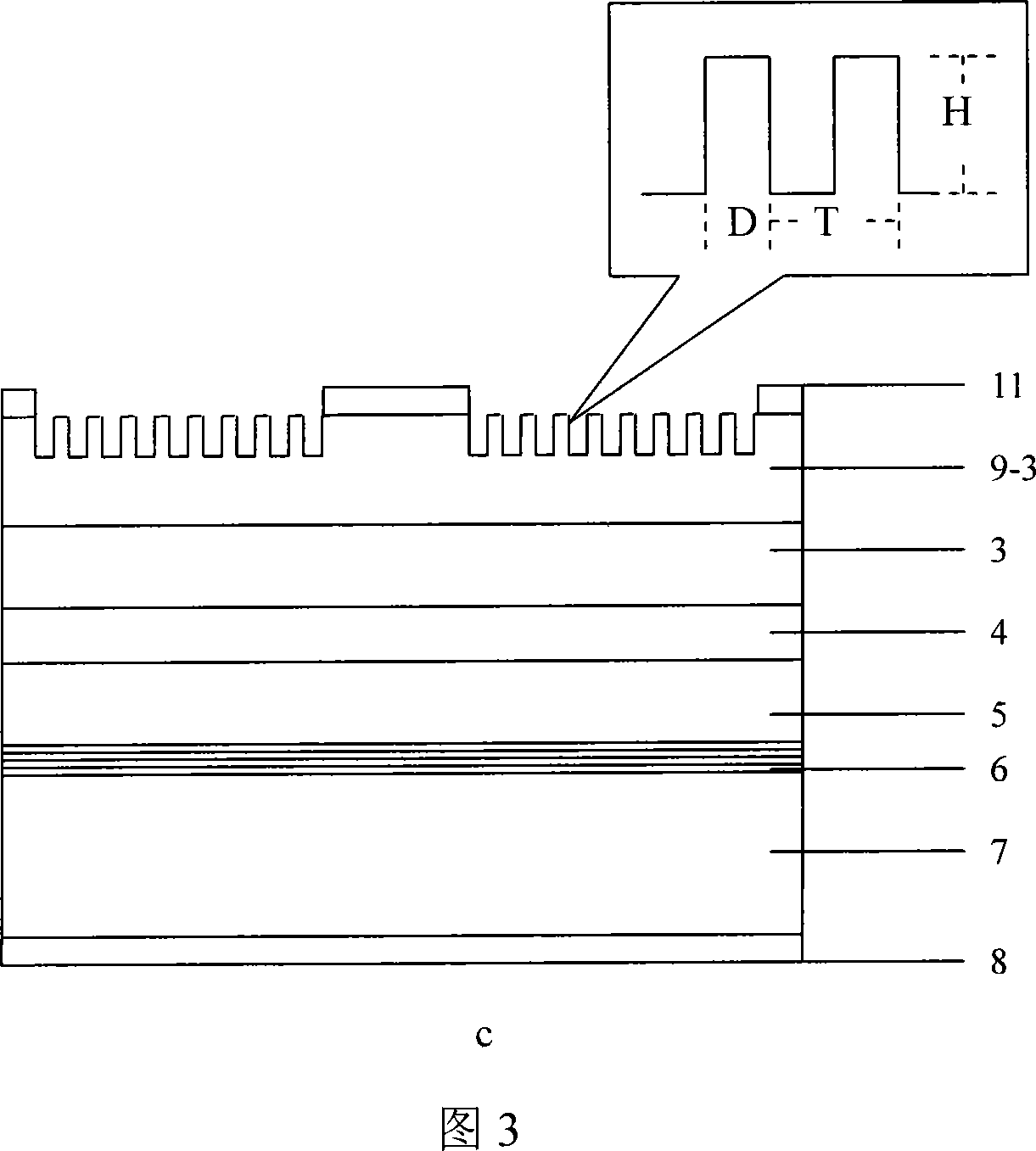
[0044] 3) Using plasma enhanced chemical vapor deposition method PECVD to grow SiO on the upper surface of GaP layer 2 2 Dielectric layer 12, as shown in Figure 4a, SiO 2 The thickness of the dielectric layer 12 is 200 Ȧ;
[0045] 4) On SiO 2 Au thin layer 13 is sputtered on dielectric layer 12, as shown in Fig. 2 In an annealing furnace in a gas environment, the temperature is 300°C, and the time is 2min, and the Au thin layer 13 is ...
Embodiment 2
[0052] 1) AlGaAs / AlAs composite Bragg reflective layer DBR 6, N-type lower confinement layer 5, multi-quantum active region 4, and P-type upper confinement layer 3 are sequentially grown on the substrate 7 by metal-organic chemical vapor deposition (MOCVD) equipment for 40 cycles and a GaP layer 2, the thickness of the GaP layer 2 is 8 μm;
[0053] 2) On the upper surface of the GaP layer 2, a P-type electrode with a grid structure of a metal frame is prepared, the plane figure is shown in Figure 5b, and the electrode size is 300 μm×300 μm;
[0054] 3) Using plasma enhanced chemical vapor deposition method PECVD to grow SiO on the upper surface of GaP layer 2 2 Dielectric layer 12, as shown in Figure 4a, SiO 2 The thickness of the dielectric layer 12 is 200 Ȧ;
[0055] 4) On SiO 2 Au thin layer 13 is sputtered on dielectric layer 12, as shown in Fig. 4a, power is 57.7W, time is 19s, the thickness of Au thin layer 13 is 25 Ȧ, put into 2 In an annealing furnace in a gas envi...
Embodiment 3
[0062] 1) AlGaAs / AlAs composite Bragg reflective layer DBR 6, N-type lower confinement layer 5, multi-quantum active region 4, and P-type upper confinement layer 3 are sequentially grown on the substrate 7 by metal-organic chemical vapor deposition (MOCVD) equipment for 40 cycles and a GaP layer 2, the thickness of the GaP layer 2 is 8 μm;
[0063] 2) On the upper surface of the GaP layer 2, a P-type electrode with a grid structure of a metal frame is prepared, the plane figure is shown in Figure 5b, and the electrode size is 300 μm×300 μm;
[0064] 3) growing an ITO dielectric layer 12 on the upper surface of the GaP layer 2 using an ITO electron beam evaporation platform, as shown in FIG. 4a, the thickness of the ITO dielectric layer 12 is 300 Ȧ;
[0065] 4) Au thin layer 13 is sputtered on the ITO dielectric layer 12, as shown in Figure 4a, the power is 57.7W, the time is 36s, the thickness of Au thin layer 13 is 50 Ȧ, put into 2 In an annealing furnace in a gas environmen...
PUM
 Abstract
Description
Claims
Application Information