Method for preparing copper-indium-sulfur semi-conductor nano particles

A nanoparticle and semiconductor technology, applied in the field of preparation of copper indium sulfur semiconductor nanoparticles, can solve the problems of non-adjustable particle size and optical properties, unsuitable for large-scale preparation, complex synthesis steps, etc., and achieve easy large-scale The effect of production, easy control and low cost

Inactive Publication Date: 2008-08-06
BAYER TECH & ENG SHANGHAI
View PDF0 Cites 25 Cited by
  • Summary
  • Abstract
  • Description
  • Claims
  • Application Information

AI Technical Summary

Problems solved by technology

However, there are several defects in the current preparation method: (1) the synthesis steps are complicated, and most of them need to pre-synthesize the precursor, which is not suitable for large-scale preparation; (2) the reactants used in the synthesis involve toxic substances; (3) the synthesis The performance of nanoparticles is poor, and the particle size and optical properties cannot be adjusted

Method used


Image

  • Method for preparing copper-indium-sulfur semi-conductor nano particles
  • Method for preparing copper-indium-sulfur semi-conductor nano particles
  • Method for preparing copper-indium-sulfur semi-conductor nano particles

Examples


Embodiment 1

[0031] Example 1. Preparation of CuInS 2 semiconductor nanoparticles

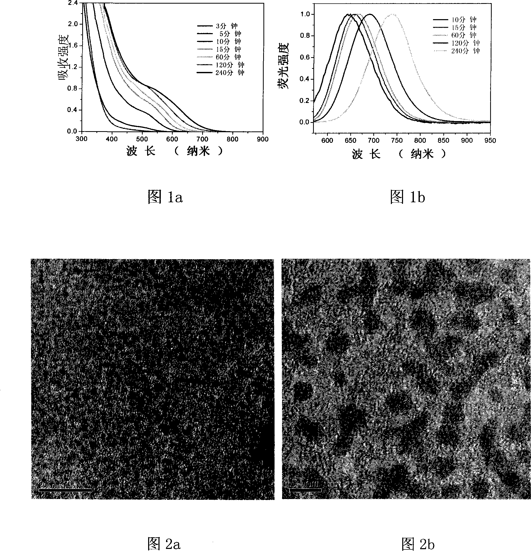
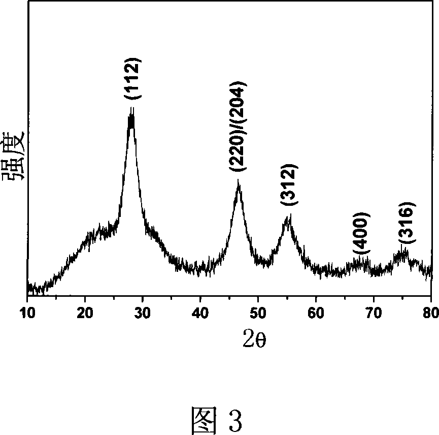
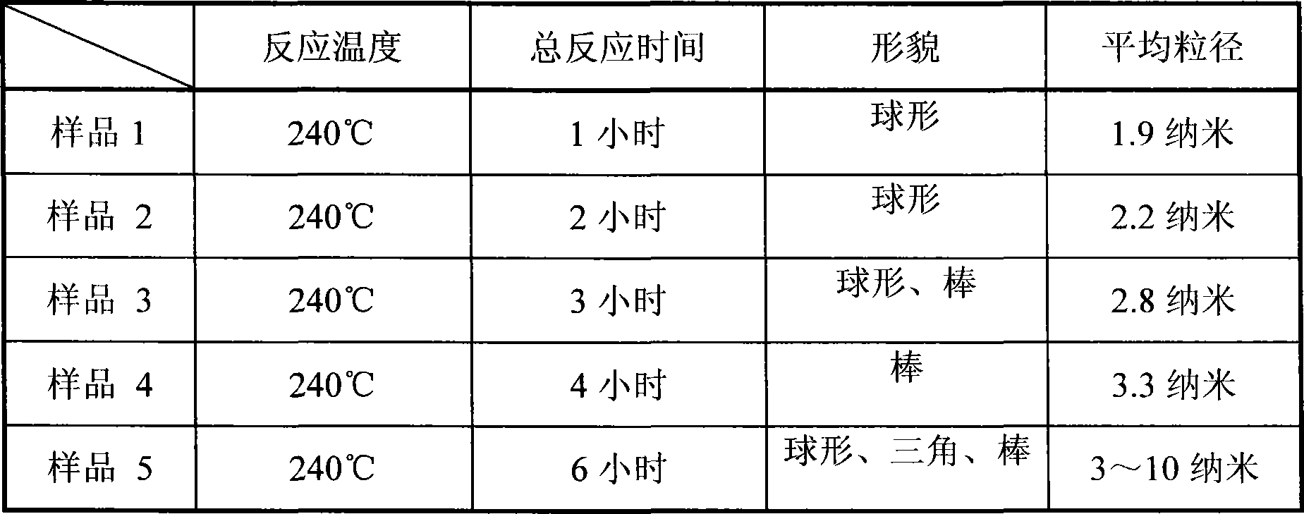
[0032] Add the mixture of cuprous acetate, indium acetate and dodecyl mercaptan and 50ml of octadecene into a 100ml three-neck flask, wherein the molar ratio of cuprous acetate, indium acetate and dodecyl mercaptan is 1:1 : 10, through argon or nitrogen for 30 minutes to get rid of the air therein, heated and stirred at 240°C to obtain a clear light yellow solution, then continued to heat the mixed solution at 240°C, the color of the colloidal solution gradually changed from light yellow to Deep red, total heating reaction time 2 hours. Cool the colloidal solution obtained from the above reaction to room temperature, add 100ml of acetone, centrifugally settle, remove the upper solution, and obtain copper indium sulfur semiconductor nanoparticles. Copper indium sulfur semiconductor nanoparticles with different shapes and sizes can be obtained by changing the reaction time (see Table 1 for specific conditio...

Embodiment 2

[0035] Example 2. Preparation of CuInS 2 semiconductor nanoparticles

[0036]Add the mixture of copper acetate, indium acetate and hexadecyl mercaptan and 25ml of octadecene into a 100ml three-neck flask, wherein the molar ratio of copper acetate, indium acetate and hexadecyl mercaptan is 1:1:10 , pass argon or nitrogen for 30 minutes to remove the air, heat and stir at 270°C to obtain a clear light yellow solution, and then continue to heat the mixed solution at a constant temperature of 270°C. The total heating reaction time is 20 minutes; a colloidal solution will be obtained The colloid solution was cooled to room temperature, 100ml of acetone was added, and the copper indium sulfur semiconductor nanoparticles with an average particle size of 3.3nm were obtained by centrifugal sedimentation.

Embodiment 3

[0037] Example 3. Preparation of CuInS 2 semiconductor nanoparticles

[0038] Add the mixture of copper acetate, indium acetate and hexadecyl mercaptan and 50ml of octadecene into a 250ml three-neck flask, wherein the molar ratio of copper acetate, indium acetate and hexadecyl mercaptan is 1:1:100 , pass argon or nitrogen for 30 minutes to remove the air, heat and stir at 240°C to obtain a clear light yellow solution, and then continue to heat the mixed solution at a constant temperature of 240°C to obtain a black sol. The total heating reaction time is 3 hours; The obtained colloidal solution was cooled to room temperature, 100 ml of acetone was added, and copper indium sulfur semiconductor nanoparticles with an average particle diameter of 3.5 nm were obtained by centrifugal sedimentation.


PUM

PropertyMeasurementUnit
particle sizeaaaaaaaaaa
particle diameteraaaaaaaaaa

Abstract

The invention relates to a method for preparing copper-indium-sulfide nano-semiconductor particle. Copper salt, indium salt and alkyl hydrosulfide are put into a reaction vessel of non-polar and high boiling organic solvent; inert gas is pumped to exclude air in the vessel; the vessel is heated, stirred and dissolved until garnet colloidal solution is obtained; the colloidal solution obtained by the step a) is cooled untill to room temperature; polar solvent is added to obtain the copper-indium-sulfide nano-semiconductor particle by centrifugal sedimentation. The copper-indium-sulfide nano-semiconductor particle can be further washed and vacuum dried to obtain copper-indium-sulfide nano-semiconductor particle powder. Particle size of the copper-indium-sulfide nano-semiconductor particle obtained by the invention is 2-10nm; morphology can be spherical, triangle, flaky and / or rod-like; productivity is up to 90 percent.

Description

technical field [0001] The invention relates to a preparation method of copper indium sulfur semiconductor nanoparticles. technical background [0002] With the development of nanotechnology, nanomaterial science has become an indispensable and important field in the development of current material science. In a sense, the progress of nanomaterial research is bound to push many disciplines such as physics, chemistry, and biology to a new level, and it will also bring new opportunities for technological research in the 21st century. As the energy problem becomes increasingly urgent, solar cells, as a renewable clean energy source, have attracted worldwide attention. Applying nanomaterials and technologies to solar cells may greatly improve the conversion efficiency of existing solar cells, reduce the production cost of solar cells, and promote the development of new solar cells. Under such circumstances, developing nanomaterials that can be used in solar cells becomes a new...

Claims


Application Information

Patent Timeline
Patent Type & Authority Applications(China)
IPC IPC(8): C01G15/00C01G3/12C01B17/20
CPCC01P2002/82C01P2002/72C01P2004/64C01P2006/40B82Y30/00C01P2004/03C01P2004/04C01G15/006Y10T428/2982
Inventor 钟海政李永舫
Owner BAYER TECH & ENG SHANGHAI
Why Eureka
Try Eureka