

Method for making high-temperature micrometre size speckle
A scale and speckle technology, applied in the field of photomechanics, can solve the problems of small application range, large speckle particles, and difficulty in controlling the speckle size, and achieve the effect of variable depth, simple process, and variable size
- Summary
- Abstract
- Description
- Claims
- Application Information
AI Technical Summary
Problems solved by technology
Method used
Image

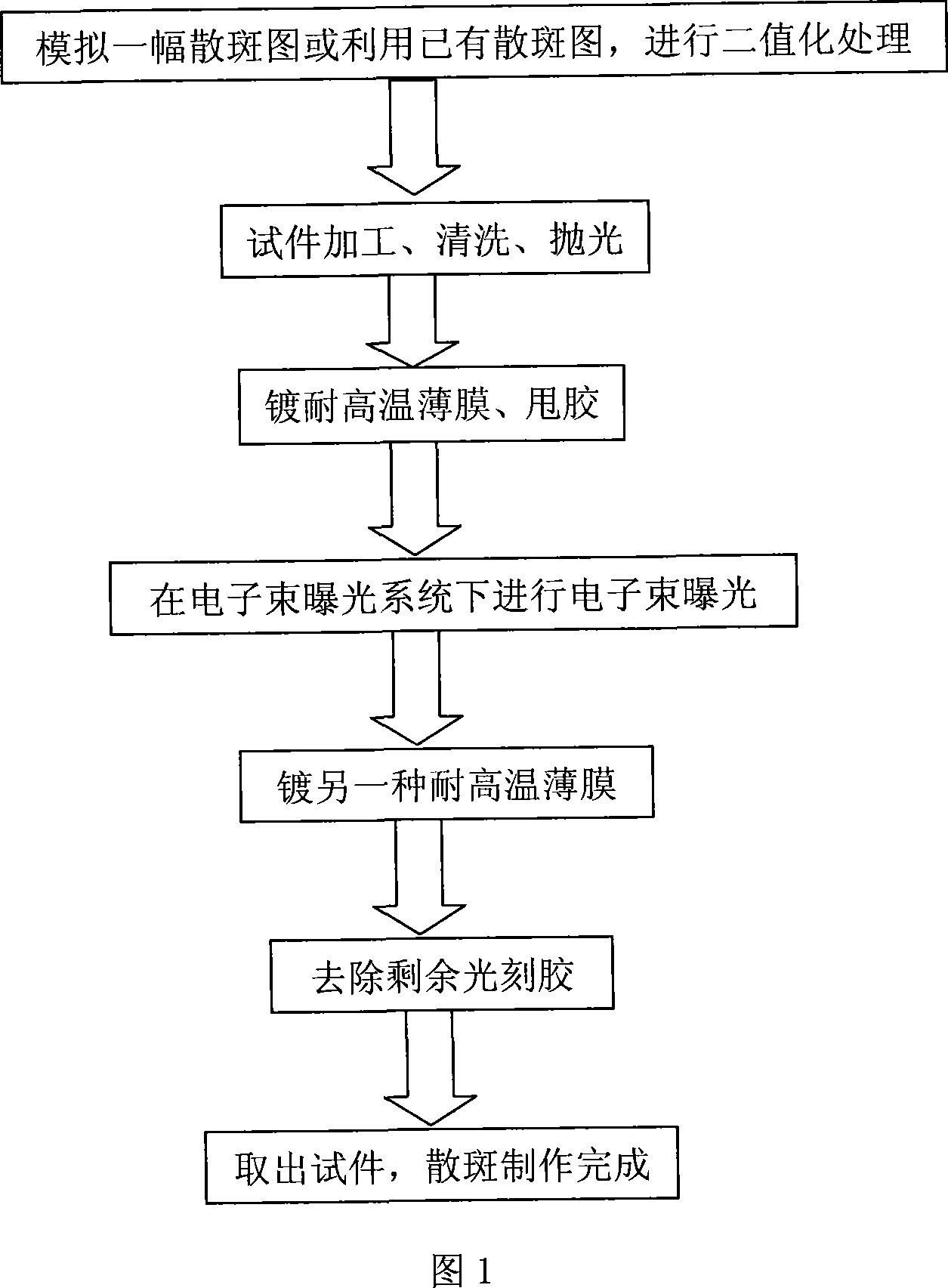
Examples
Embodiment 1
[0022] The material of the test piece is a single crystal silicon wafer. After cleaning, a layer of Au film with a thickness of 0.5 μm is coated on the surface of the test piece, and a layer of ZEP520A photoresist with a thickness of 0.5 μm is uniformly coated on the glue machine.
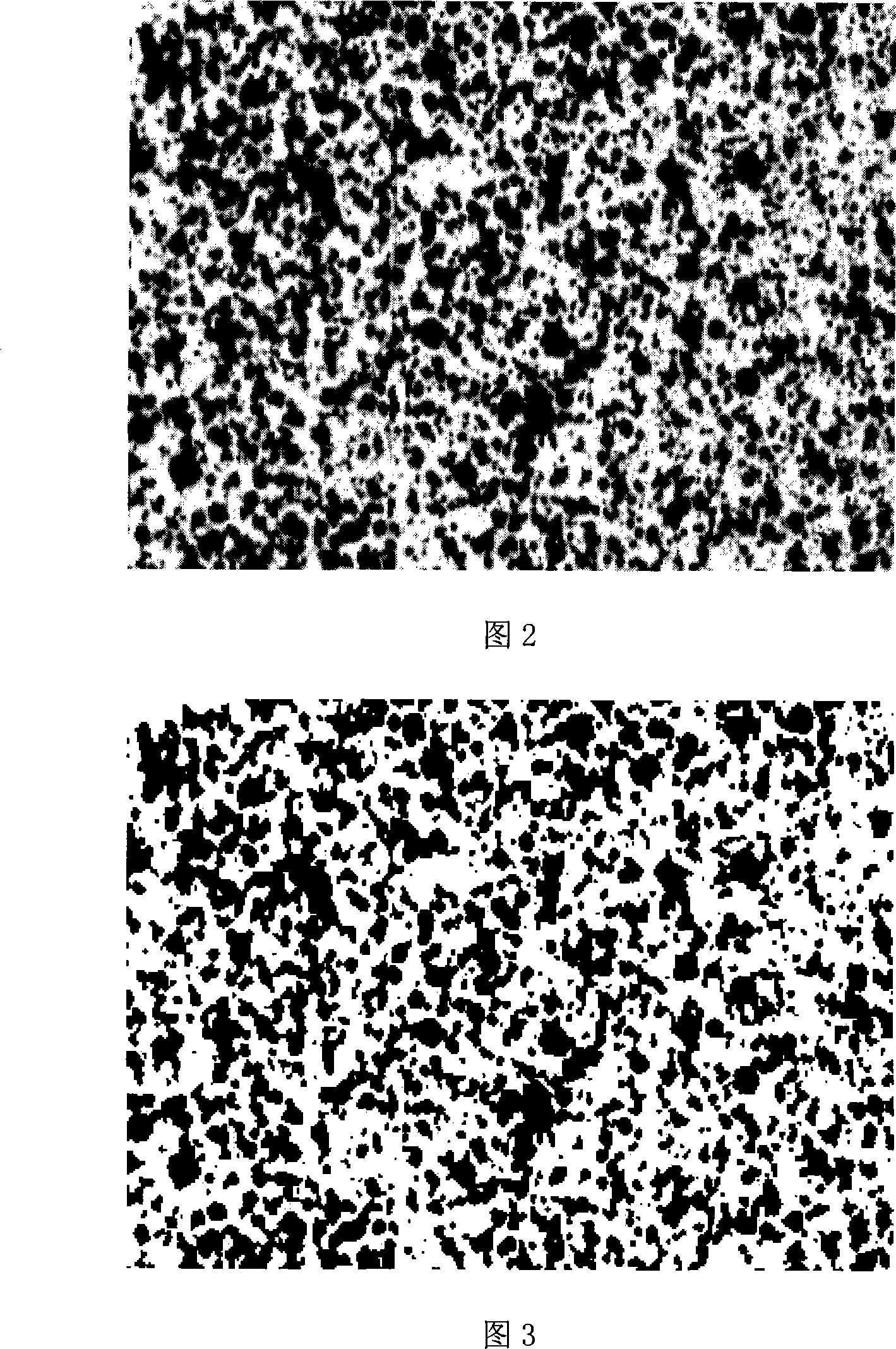
[0023] The test piece is placed on the stage of the electron beam exposure machine, so that the side coated with Au film faces upwards. After repeated attempts to optimize the selection, the acceleration voltage U=20kV, the beam intensity I=430nA, and the magnification are 500, the working distance is 30mm, open the binary image (Figure 3) converted from the simulated speckle image (Figure 2), the exposure time is 10s, and the developer and fixer used are ZED-N50 and 2propand (isopropyl Alcohol) with a volume ratio of 2:3, and then plated with a Cr film with a thickness of 0.3um. After degumming, the desired speckle pattern is finally obtained.
Embodiment 2
[0025] The material of the test piece is a glass sheet. After cleaning, a layer of Ag film is coated on the surface of the test piece with a thickness of 0.3 μm, and a layer of ZEP520A photoresist is uniformly coated on the glue machine with a thickness of 0.5 μm.
[0026] The test piece is placed on the stage of the electron beam exposure machine, so that the side coated with the Ag film faces upwards. After repeated attempts to optimize the selection, the acceleration voltage U=15kV is selected, the beam intensity I=200nA, and the magnification is 1000, the working distance is 25mm, open the binary image (Figure 3) converted from the simulated speckle image (Figure 2), the exposure time is 15s, and the developer and fixer used are ZED-N50 and 2propand (isopropyl Alcohol) with a volume ratio of 2:3, and then plated with a Cu film with a thickness of 0.2 μm, and finally obtained the required speckle pattern after degumming.
Embodiment 3
[0028] The material of the test piece is a single crystal silicon wafer. After cleaning, a layer of SiO is coated on the surface of the test piece. 2 film, with a thickness of 0.1 μm, and uniformly coat a layer of ZEP520A photoresist on a glue spinner with a thickness of 0.1 μm.
[0029] The specimen was placed on the stage of the electron beam exposure machine, so that it was coated with SiO 2 One side of the film is facing upwards, after repeated attempts to optimize the selection, select the acceleration voltage U=10kV, the beam intensity I=100nA, the magnification factor is 2000, the working distance is 18mm, and the opening is converted from the simulated speckle pattern (Figure 2). The binary image (Figure 3) was exposed after clear focus, the exposure time was 8s, the developer and fixer used were ZED-N50 and 2propand (isopropanol) respectively, the volume ratio was 2:3, and then silicon nitride was plated The film, with a thickness of 0.1 μm, is finally degummed to ob...
PUM
| Property | Measurement | Unit |
|---|---|---|
| Film thickness | aaaaa | aaaaa |
Abstract
Description
Claims
Application Information