Realizing method of novel enhancement type AlGaN/GaN HEMT device

An implementation method and enhanced technology, applied in the field of microelectronics, can solve the problems of device performance and reliability impact, insufficient threshold voltage, low threshold voltage, etc., and achieve high device reliability, high depletion rate, and low cost.

Inactive Publication Date: 2008-08-27
XIDIAN UNIV
View PDF0 Cites 28 Cited by
  • Summary
  • Abstract
  • Description
  • Claims
  • Application Information

AI Technical Summary

Problems solved by technology

There are still great shortcomings in the existing technology. First, the threshold voltage is not high. The highest reported value is only 0.9V, which is far from enough for switching applications. Second, whether etching to form grooves or fluorine ion implantation will affect the material Although some damage can be eliminated after annealing, the residual damage will still affect the performance and reliability of the device. At the same time, the repeatability of this process is not high; the third is to form short-channel devices for microwave applications. High-end process equipment such as electron beam direct writing is required to produce short gate lengths, and the process is difficult

Method used


Image

  • Realizing method of novel enhancement type AlGaN/GaN HEMT device
  • Realizing method of novel enhancement type AlGaN/GaN HEMT device
  • Realizing method of novel enhancement type AlGaN/GaN HEMT device

Examples


Embodiment Construction

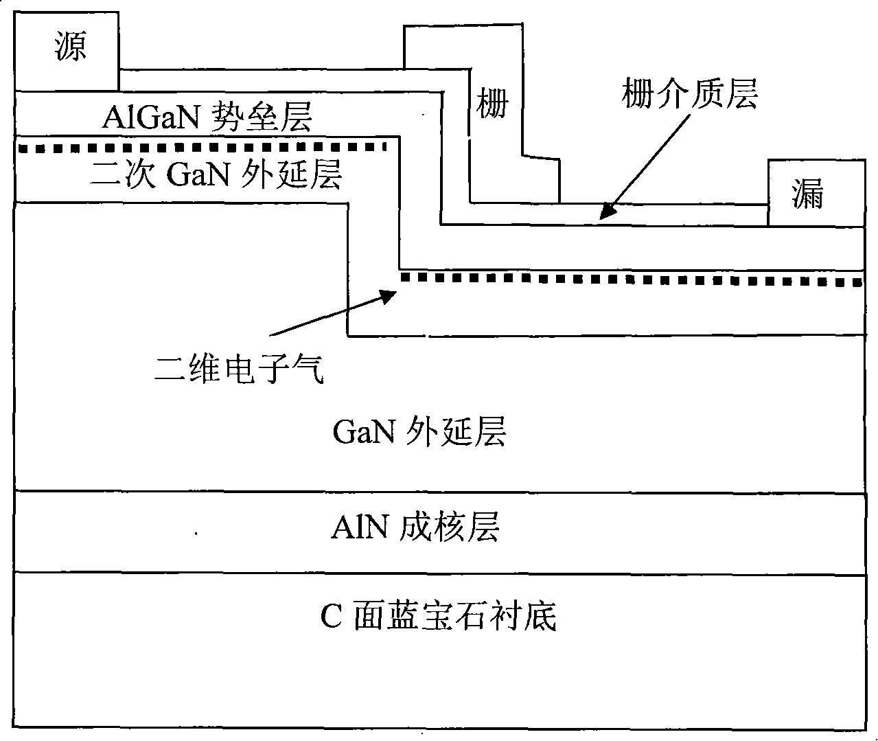
[0034] see figure 1 , which is a schematic cross-sectional structure diagram of the single-gate enhanced AlGaN / GaN HEMT device completed in Embodiment 1 of the present invention. In this embodiment, a 0001-plane sapphire substrate is selected as the growth substrate, and a single-gate enhanced AlGaN / GaN HEMT device is prepared according to the following process:

[0035] 1. Put the sapphire substrate in the reaction chamber of the metal organic chemical vapor deposition MOCVD equipment, and pump the vacuum degree of the reaction chamber to 1×10 -2 Under Torr, the sapphire substrate is subjected to high-temperature heat treatment and surface nitriding under the protection of a mixed gas of hydrogen and ammonia. The heating temperature is 1050°C, the heating time is 5min, the pressure of the reaction chamber is 40Torr, and the flow rate of hydrogen gas is 1500sccm. Ammonia flow rate is 1500sccm;

[0036] 2. Lower the substrate temperature to 500°C, keep the growth pressure at ...


PUM


Abstract

The invention discloses a realization method for a novel enhancement type AlGaN/GaN HEMT device, relating to the microelectronic technical field. The realization method has low cost, simple technique, good repeatability, high reliability and small damage on materials. The enhancement type HEMT device with high threshold voltage and nano-sized effective channel length can be obtained. The invention adopts the method of etching a table top after growth of an AlN nucleating layer and a GaN epitaxial layer and before growth of a secondary GaN epitaxial layer and an AlGaN layer to make heterojunction materials on the side face of the table top grow along the nonpolarized direction, thereby the air density of two-dimensional electrons in the heterojunction materials on the side face of the table top is greatly reduced. A grid electrode of the device is produced on the side face of the table top; under the condition of no additional voltage on the grid electrode, a conductive channel can not be switched on or weakly switched on; under the condition of certain additional positive bias on the grid electrode, the conductive channel is switched on. The invention can be used in a high-temperature high-frequency high-power situation, a high-power switch and a digital circuit.

Description

technical field [0001] The invention belongs to the technical field of microelectronics, and relates to semiconductor materials and device manufacturing technology. Specifically, it is a realization method of a new enhanced AlGaN / GaN HEMT device, which can be used in high-temperature, high-frequency, high-power occasions, high-power switches, and digital circuits. Background technique [0002] As a typical representative of wide bandgap semiconductor materials, GaN-based materials have the characteristics of large bandgap width, high electron saturation drift velocity, high breakdown field strength and good thermal conductivity, and can be used to make high-temperature, high-frequency and high-power electronic devices. More importantly, GaN-based materials can form modulation-doped AlGaN / GaN heterostructures, which can obtain high electron mobility, extremely high peak electron velocity and saturation electron velocity at room temperature, and obtain better than the first H...

Claims


Application Information

Patent Timeline
Patent Type & Authority Applications(China)
IPC IPC(8): H01L21/335
Inventor 张进城郑鹏天郝跃董作典王冲张金风吕玲秦雪雪
Owner XIDIAN UNIV
Why Eureka
Try Eureka