Nanometer silicon hetero-junction bidirectional tunneling diode

A technology of tunneling diodes and nano-silicon, which is applied in diodes, electrical components, circuits, etc., can solve the problems of weak withstand voltage and limit the application field of diodes, and achieve the effect of improving withstand voltage.

Inactive Publication Date: 2008-09-03
韦文生
View PDF0 Cites 4 Cited by
  • Summary
  • Abstract
  • Description
  • Claims
  • Application Information

AI Technical Summary

Problems solved by technology

For example, the reverse current-voltage (I-V) curve of the nano-silicon heterojunction diode introduced in "Resonant Tunneling Phenomenon in Nano-Silicon Thin Film Diodes" in the 23rd issue of 1998 in the Journal of Semiconductors shows that the current of the reverse current-voltage (I-V) curve is stepped, which shows that the carrier resonant tunneling , but there is no different

Method used


Image

  • Nanometer silicon hetero-junction bidirectional tunneling diode
  • Nanometer silicon hetero-junction bidirectional tunneling diode
  • Nanometer silicon hetero-junction bidirectional tunneling diode

Examples


specific Embodiment approach 2

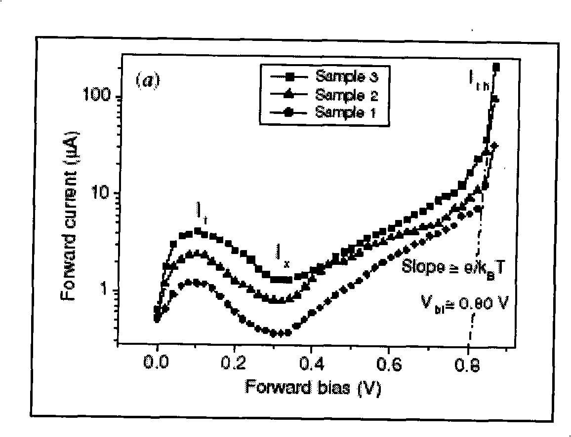
[0021] Specific embodiment 2 (preparation sample Sample 2): differ from embodiment 1 in that the gaseous phase dopant during the preparation of the described phosphorus-doped nano-silicon film is phosphine, which is used when preparing the nano-silicon film. The proportion of silane is 0.5 vol% by volume.

specific Embodiment approach 3

[0022] Specific embodiment 3 (preparation sample Sample 3): differ from embodiment 1 in that the gas phase dopant during the preparation of the described phosphorus-doped nano-silicon film is phosphine, which is used when preparing the nano-silicon film. The proportion of silane is 1.0 vol% by volume.

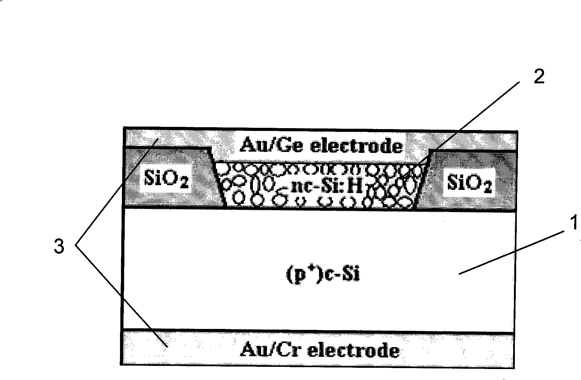
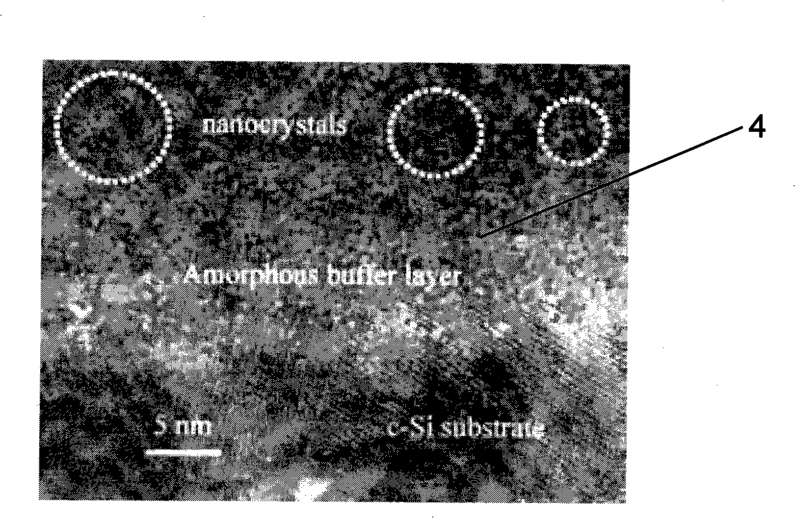
[0023] The manufacturing process of the present invention is: select about 100 μ m thick, the average carrier concentration is at 10 18 -10 19 cm -3 The monolithic polished p+ type crystalline silicon (111) wafer is used as the substrate material. First, the substrate wafer is prepared with about 100 nm thick SiO by heating oxidation method at 1020 °C. 2 Floor. SiO by photolithography 2 A series of 30 μm × 30 μm square windows are etched out of layers, and then a layer of fresh n-type nc-Si:H film is deposited in these windows by plasma enhanced chemical vapor deposition (PECVD), and then the square windows are removed by photolithography. For the outer nc-Si:H film, only...


PUM

PropertyMeasurementUnit
Particle sizeaaaaaaaaaa
Thicknessaaaaaaaaaa
Thicknessaaaaaaaaaa

Abstract

The present invention discloses a nano silicon hetero-junction bidirectional tunnel diode which includes a monocrystalline silicon substrate, a electric pole, a nano silicon thin film deposited at the monocrystalline silicon substrate includes nano silicon grain embedded in the hydrogenization amorphism silicon organize, the nano silicon thin film and the heterojunction structure configured with the nano silicon monocrystalline silicon, which is characterized in that the grain diameter of the nano silicon grain is 4-6nm, and the grain diameter sizes of different nano silicon grain are approach. The present invention has differential coefficient dynatron effect caused by the forward bias tunnel, meanwhile also has sequence resonance tunnel phenomenon of quantization energy level of multi- nanocrystal under back bias voltage, in addition breakdown reverse voltage is improved greatly to arrive more than -37V.

Description

technical field [0001] The present invention relates to a quantum device with a heterostructure, more specifically a heterojunction tunneling diode, in particular to a sequence in which the forward direction is inter-band tunneling and the reverse direction is the quantum energy level of nano-silicon crystal grains. Resonant tunneling properties of nano-silicon heterojunction bidirectional tunneling diodes. Background technique [0002] Tunnel diodes can be used in local oscillators and phase-locked circuits of low-power microwave circuits, and in reverse tunnel diodes can be used in small-signal rectification, microwave frequency detection and frequency mixing circuits. Hydrogenated nanocrystalline silicon (nc-Si:H) thin films, composed of nanocrystalline silicon grains embedded in a hydrogenated amorphous (a-Si:H) structure, have attracted attention due to their potential applications in microelectronic and optoelectronic integration. extensive attention. For example, th...

Claims


Application Information

Patent Timeline
IPC IPC(8): H01L29/88H01L29/04
Inventor 韦文生
Owner 韦文生
Why Eureka
Try Eureka