Method for preparing transistor T type nano grid

A manufacturing method and transistor technology, which are applied in semiconductor/solid-state device manufacturing, semiconductor devices, electrical components, etc., can solve the problems of difficult process realization and extremely high requirements for overlay accuracy, and achieve easy control of development time, high reliability, and high reliability. simple craftsmanship

Inactive Publication Date: 2008-10-01
INST OF MICROELECTRONICS CHINESE ACAD OF SCI
View PDF0 Cites 7 Cited by
  • Summary
  • Abstract
  • Description
  • Claims
  • Application Information

AI Technical Summary

Problems solved by technology

This method requires extremely high overlay accuracy between the grid cap plate and the grid foot plate, and it is difficult to realize the process

Method used


Image

  • Method for preparing transistor T type nano grid
  • Method for preparing transistor T type nano grid
  • Method for preparing transistor T type nano grid

Examples


Embodiment

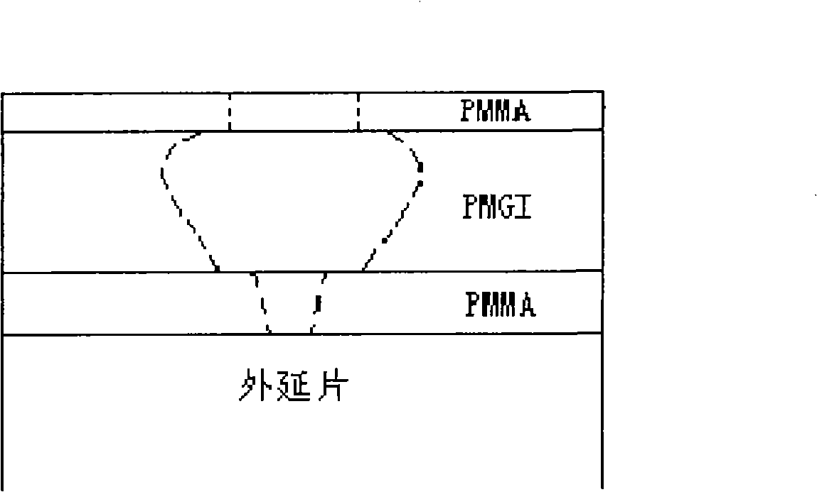
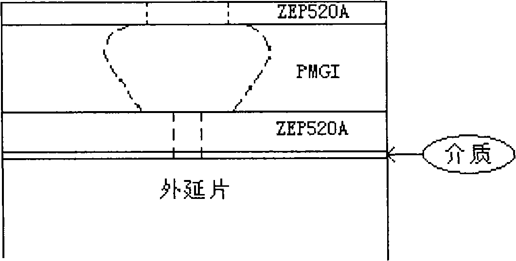
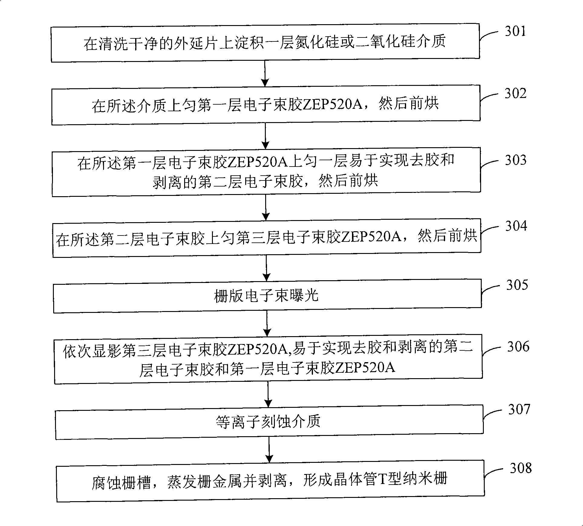
[0070] The method for fabricating the T-type nano-gate of the high electron mobility transistor (HEMT) in this embodiment is to address some shortcomings in the production of the T-type nano-gate of the high electron mobility transistor (HEMT) at present, using ZEP520A / PMGI / ZEP520A three-layer electron beam The photoresist structure (as shown in Table 1) and one electron beam exposure method are used to fabricate the T-type nano-gate of high electron mobility transistor (HEMT).

[0071] Table 1 is a schematic diagram of the structure of the ZEP520A / PMGI / ZEP520A three-layer electron beam photoresist used in the method for manufacturing the T-type nano-gate of the high electron mobility transistor (HEMT) of the present invention:

[0072]

[0073] Table 1

[0074] In this embodiment, the second layer of electron beam glue that is easy to remove and peel off is PMGI electron beam glue, and the ZEP520A / PMGI / ZEP520A three Layer electron beam photoresist structure, the role of e...


PUM


Abstract

The invention discloses a method for manufacturing transistor T-shaped nanometer gate, comprising the steps of: A, depositing a layer of silicon nitride medium or silicon dioxide medium on a cleaned epitaxial wafer; B, coating a first layer electric beam glue ZEP520A on the silicon nitride medium or silicon dioxide medium, and then soft-baking; C, coating a second layer electric beam glue which is liable to realize glue-stripping and peeling on the first layer electric beam glue ZEP520A, and then soft-baking; D, coating a third layer electric beam glue ZEP520A on the second layer electric beam glue, and then soft-baking; E, carrying out gate electric beam exposure; F, sequentially developing the third layer electric beam glue ZEP520A, the second layer electric beam glue which is liable to realize glue-stripping and peeling and the first layer electric beam glue ZEP520A; G, plasma-etching the silicon nitride medium or silicon dioxide medium; H, eroding the gate groove, evaporating and peeling off gate metals to form the transistor T-shaped nanometer gate. In free of the problem about overlaying alignment, the invention is simple in processes, easy to manufacture the gate lines having small size and strong in reliability.

Description

technical field [0001] The invention relates to the technical field of compound semiconductors, in particular to a method for manufacturing a T-shaped nano-gate of a high electron mobility transistor. Background technique [0002] Gate fabrication is the most critical process in the high electron mobility transistor (HEMT) device fabrication process. Since the gate length directly determines the frequency, noise and other characteristics of the HEMT device, the smaller the gate length, the current cutoff frequency of the device (f T ) and power gain cutoff frequency (f max ) The higher the noise figure of the device is, the smaller the noise figure of the device is. People can obtain devices with better characteristics by continuously reducing the gate length of high electron mobility transistor (HEMT) devices. [0003] As the gate length shortens, the gate resistance increases, and when the gate length decreases below 0.5 μm, the microwave loss of the gate resistance make...

Claims


Application Information

Patent Timeline
Patent Type & Authority Applications(China)
IPC IPC(8): H01L21/28H01L21/335
Inventor 刘亮张海英刘训春
Owner INST OF MICROELECTRONICS CHINESE ACAD OF SCI
Why Eureka
Try Eureka