Method for growing high quality nano-diamond membrane with low cost

A nano-diamond, high-quality technology, applied in metal material coating process, gaseous chemical plating, coating, etc., can solve the problems of poor reusability, high preparation cost and limited life of hot wire, and achieve unique field emission advantages , The effect of low preparation cost and large excitation current

Inactive Publication Date: 2008-10-29
MUDANJIANG NORMAL UNIV
View PDF0 Cites 17 Cited by
  • Summary
  • Abstract
  • Description
  • Claims
  • Application Information

AI Technical Summary

Problems solved by technology

Microwave plasma CVD equipment is relatively complex and expensive, while the hot wire CVD

Method used


Image

  • Method for growing high quality nano-diamond membrane with low cost
  • Method for growing high quality nano-diamond membrane with low cost
  • Method for growing high quality nano-diamond membrane with low cost

Examples


specific Embodiment approach 1

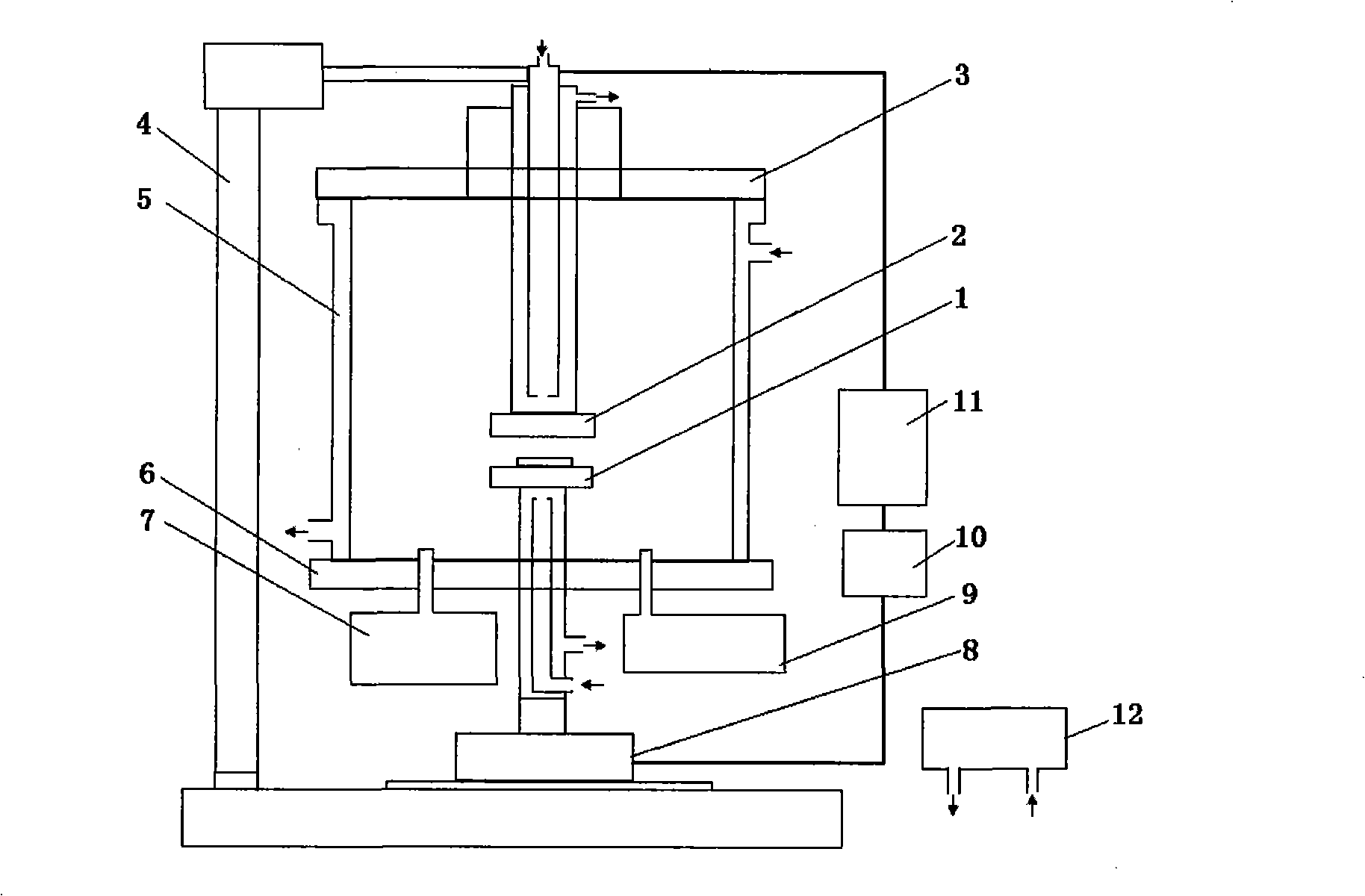
[0014] Specific implementation mode one: as figure 1 As shown, the present embodiment prepares the nano-diamond film in the equipment for growing high-quality nano-diamond film at low cost. System 12. The cathode 2 is fixed at the center position of the end cap 3, and the cathode 2 and the end cap 3 can be raised and lowered under the traction of the end cap lifting device 4, so that the growth chamber 5 is opened or closed; the anode 1 is raised and lowered under the traction of the anode lifting device 8; The air intake device 7 and the vacuum device 9 communicate with the growth chamber at the lower end cover 6 of the growth chamber 5; through the adjustment of the voltage regulator 10, the voltage output from the power supply 11 to the cathode 2 and the anode 1 is changed; the water cooling system 12 is respectively It communicates with the wall of the cathode 2, the anode 1 and the growth chamber 5, and the water cooling channels communicate with each other. The distanc...

specific Embodiment approach 2

[0024] Specific implementation mode 2: In this implementation mode, a low-cost and high-quality nano-diamond film is prepared according to the following method:

[0025] a. Ultrasonic grinding of the Si sheet with diamond powder for 1 h, ultrasonic cleaning with ethanol for 1 h, drying and putting it on the anode platform in the growth chamber. After the descending end cap is sealed, the growth chamber is evacuated to 10 -1 Pa, close the main valve for vacuuming, open the flow meter and fill it with H with a flow rate of 200-300 sccm 2 . Adjust the position of the anode close to the cathode by about 20mm, and wait for the air pressure in the growth chamber to rise to 0.8×10 3 Pa, add voltage, adjust the working voltage, so that the electrode can reach a stable glow discharge state.

[0026] b. After the discharge is stable, charge H with a flow rate of 200 sccm 2 , CH at 10 sccm 4 , keep the growth chamber pressure at 1.2×10 4 Pa, Si sheet temperature 850°C, excitation v...


PUM


Abstract

The invention relates to a method for producing high-quality nano-diamond film with low cost, which belongs to the superhard material growth field. The method takes hydrogen, argon and carbonaceous gas as the precursor gas, plasma is formed by utilizing hot cathode glow discharge excitation, the diamond film nucleation and growth can be alternately performed through controlling the gas supply proportion, the diamond crystal particles are controlled within the nanometer range, and high-quality nano-diamond film is deposited after mainly going through the process of nucleation, nano-diamond film deposition and removal of the non-diamond phase carbon on the surface of the film. The method for producing the high-quality nano-diamond film with low cost has the advantages of high excitation current, quick growth speed, high film forming quality and low preparation cost; the prepared nano-diamond film also has the advantages of low surface roughness, small friction coefficient and low electrical resistivity besides excellent physical and chemical properties of the conventional diamond; the surface grain size is 10 to 100 nm.

Description

technical field [0001] The invention belongs to the field of superhard material growth, and relates to a method for preparing a nano-diamond film. Background technique [0002] Usually, the diamond film grown by chemical vapor deposition method (referred to as CVD) has almost the same properties as single crystal diamond. This kind of diamond film is composed of micron-scale (several microns to tens of microns) columnar polycrystals, and the growth surface is relatively rough. The high hardness and high wear resistance of diamond make it extremely difficult to flatten and polish the film; due to the resistivity of diamond Very high (resistivity 10 9 -10 16 ), and cannot be polished and cut by electric machining; the diaphragm has a large particle size, and it is difficult to make it into a small component with high shape accuracy. The disadvantages of micron-scale diamond films have seriously affected the applications of diamond films in machining, optics and electronics....

Claims


Application Information

Patent Timeline
IPC IPC(8): C23C16/27C23C16/513C23C16/455C23C16/52
Inventor 彭鸿雁陈玉强赵立新姜宏伟
Owner MUDANJIANG NORMAL UNIV
Why Eureka
Try Eureka