

Production method of bulk silicon nano line transistor device
A technology of silicon nanowires and transistors, which is applied in the field of field effect transistor preparation, can solve the problems of small cross-section of source and drain regions, process complexity, and reduce device drive current, so as to reduce process manufacturing cost and have strong process controllability , Reduce the effect of parasitic resistance
- Summary
- Abstract
- Description
- Claims
- Application Information
AI Technical Summary
Problems solved by technology
Method used
Image

Examples
Embodiment Construction
[0040] The present invention will be described in detail below with reference to the accompanying drawings and specific embodiments, and a specific process scheme for realizing the silicon nanowire structure proposed by the present invention will be given.
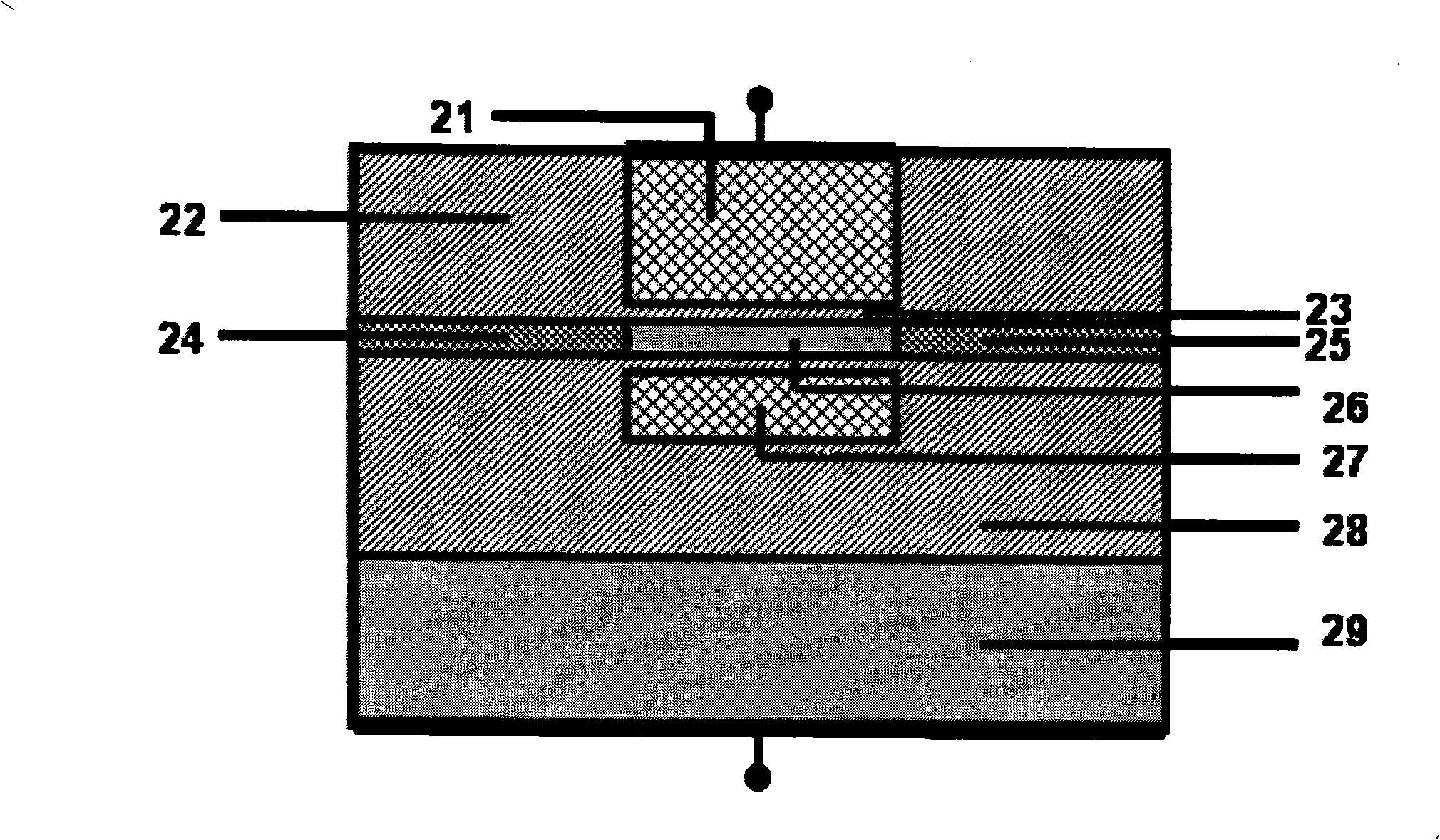
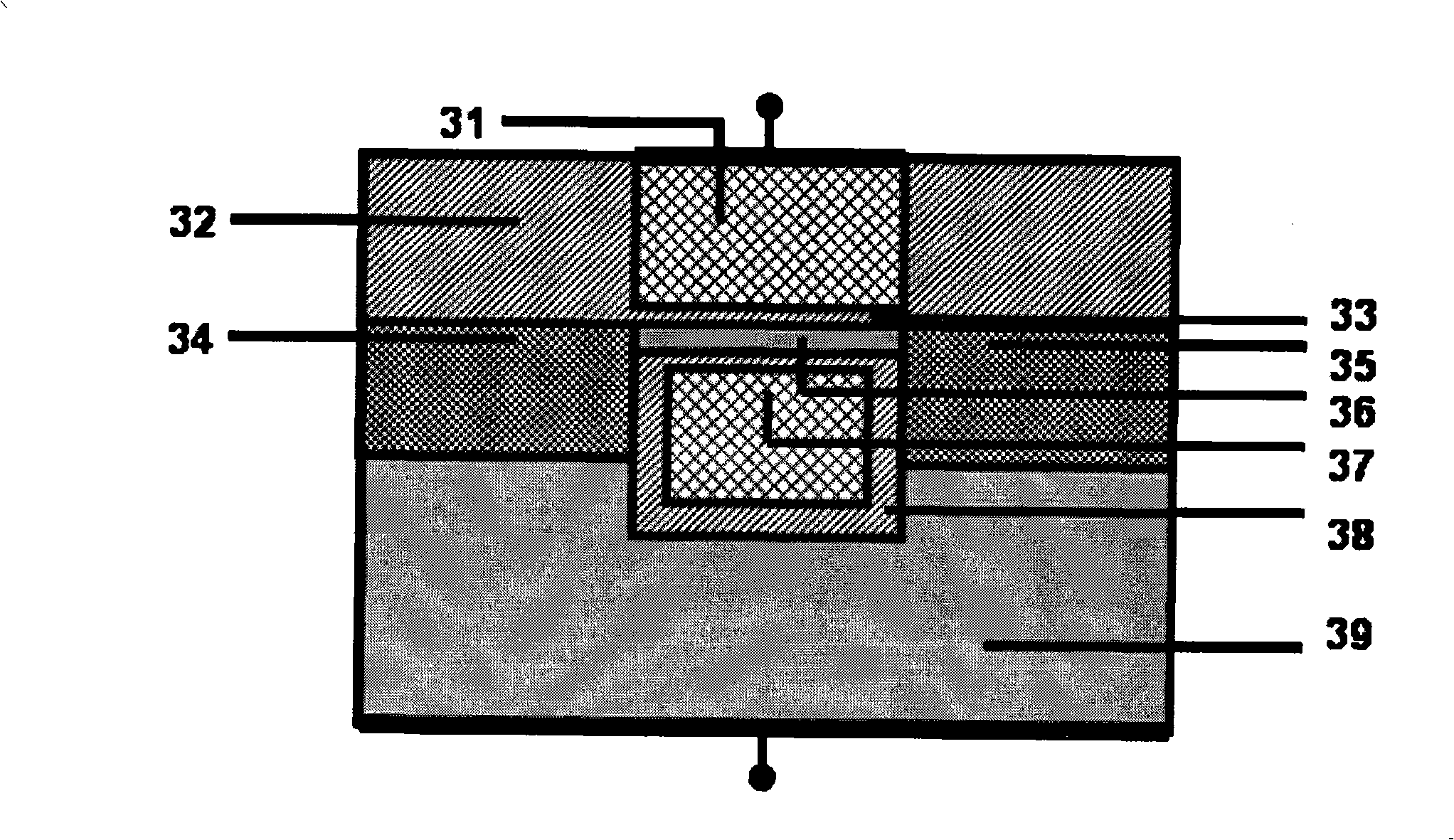
[0041] 1. Preparation, traditional bulk silicon wafer, such as Figure 4 (a).
[0042] 2. Utilize the traditional shallow trench isolation (STI-shallow trench isolation) isolation method.
[0043] 3. Chemical vapor deposition (LPCVD) silicon oxide
[0044] 4. Chemical vapor deposition (LPCVD) silicon nitride
[0045] 5. Electron beam lithography nanowires.
[0046] 6. Reactive ion etching (RIE) etching silicon oxide
[0047] 7. Reactive ion etching (RIE) etching silicon nitride Such as Figure 4 (b).
[0048] 8. Remove glue and clean.
[0049] 9. Chemical Vapor Deposition (LPCVD) Silicon Oxide
[0050] 10. Etching silicon oxide by reactive ion etching (RIE) Such as Figure 4 (c)
[0051] 11. Arsenic z...
PUM
 Abstract
Description
Claims
Application Information