Process for preparing manganic manganous oxide nanometer wire by vapor deposition
A nanometer and vapor deposition technology of manganese tetroxide, applied in chemical instruments and methods, from condensed steam, single crystal growth, etc. Effect
- Summary
- Abstract
- Description
- Claims
- Application Information
AI Technical Summary
Problems solved by technology
Method used
Image
Examples
Embodiment 1
[0017] 1. Collect Mn by using silicon wafer coated with gold film 3 o 4 Nanowires. Before preparation, the coated silicon wafers were ultrasonically cleaned with acetone and then rinsed with deionized water.
[0018] 2. Place the high-purity Mn powder in an aluminum oxide crucible, cover the cleaned silicon chip directly above the Mn source, and the vertical distance between the silicon chip and the evaporation source is 1 mm. Put them together in a horizontal tube furnace.
[0019] 3. Raise the furnace temperature to 950°C and keep it warm for 2 hours. Argon gas with a flow rate of 145 ml / min was filled throughout the growth process. Cool down to room temperature naturally after growth.
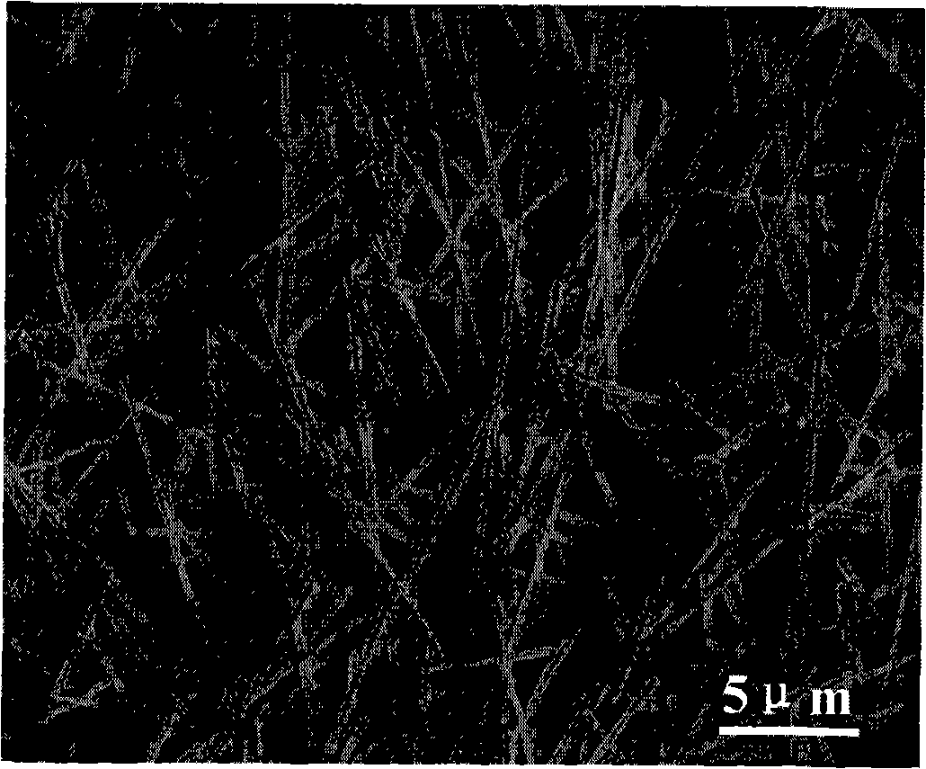
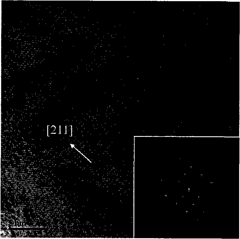
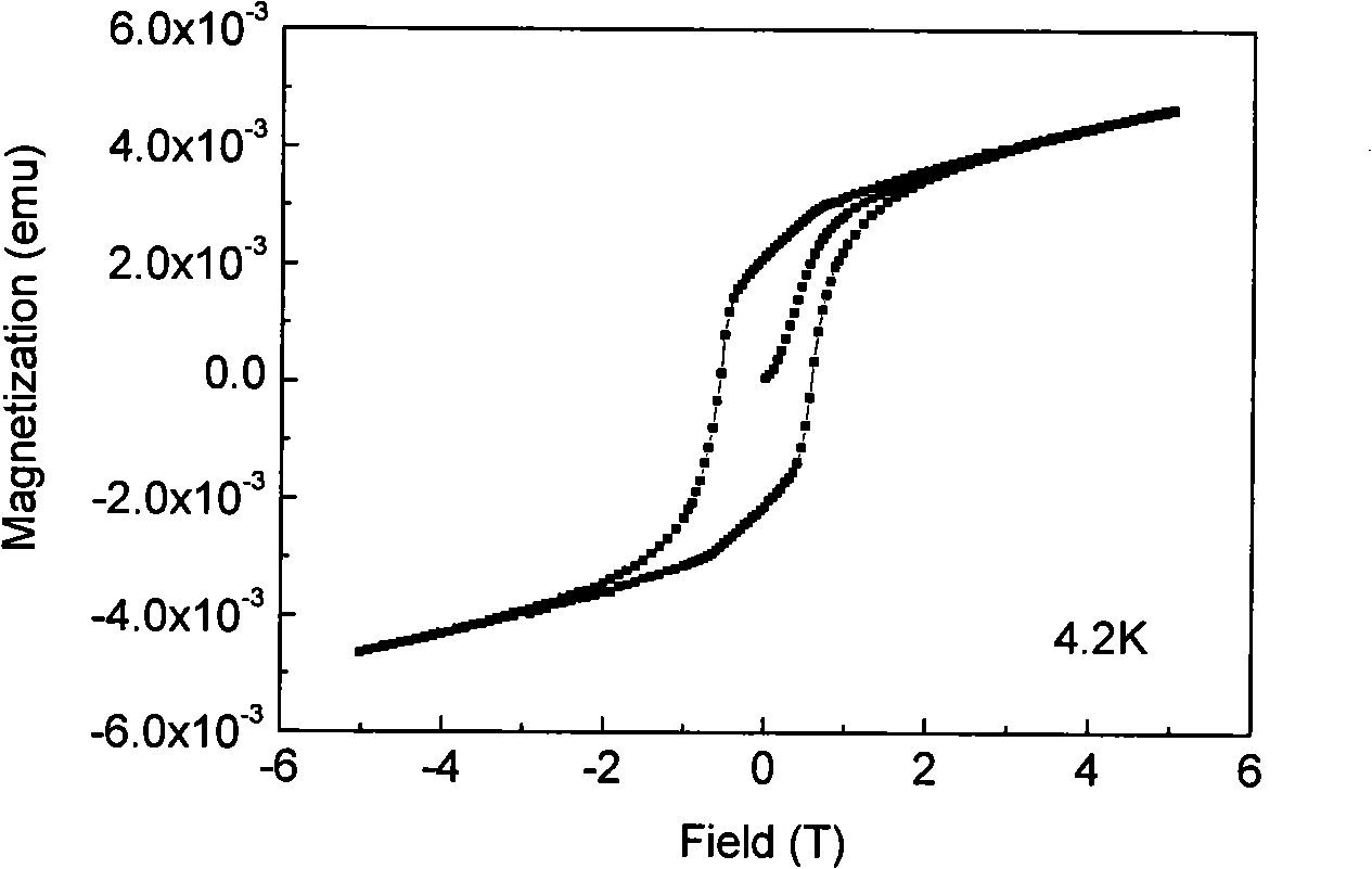
[0020] The sample was observed with a scanning electron microscope, and it was found that a thick layer of nanowires was uniformly deposited on the silicon substrate. The nanowires were relatively straight and of high purity, and no particles were observed (Figure 1). Figure 2 is a tra...
Embodiment 2
[0022] 1. Collect Mn by using silicon wafer coated with gold film 3 o 4 Nanowires. Before preparation, the coated silicon wafers were ultrasonically cleaned with acetone and then rinsed with deionized water.
[0023] 2. Place the high-purity Mn powder in an aluminum oxide crucible, cover the cleaned silicon chip directly above the Mn source, and the vertical distance between the silicon chip and the evaporation source is 2 mm. Put them together in a horizontal tube furnace.
[0024] 3. Raise the furnace temperature to 1000°C and keep it warm for 2 hours. Argon gas with a flow rate of 150ml / min was filled throughout the growth process. Cool down to room temperature naturally after growth.
Embodiment 3
[0026] 1. Collect Mn by using silicon wafer coated with gold film 3 o 4 Nanowires. Before preparation, the coated silicon wafers were ultrasonically cleaned with acetone and then rinsed with deionized water.
[0027] 2. Place the high-purity Mn powder in an aluminum oxide crucible, cover the cleaned silicon chip directly above the Mn source, and the vertical distance between the silicon chip and the evaporation source is 1 mm. Put them together in a horizontal tube furnace.
[0028] 3. Raise the temperature of the furnace to 900°C and keep it warm for 4 hours. Argon gas with a flow rate of 50 ml / min was filled throughout the growth process. Cool down to room temperature naturally after growth.
PUM
| Property | Measurement | Unit |
|---|---|---|
| Coercivity | aaaaa | aaaaa |
Abstract
Description
Claims
Application Information
 - R&D Engineer
- R&D Manager
- IP Professional
- Industry Leading Data Capabilities
- Powerful AI technology
- Patent DNA Extraction
Browse by: Latest US Patents, China's latest patents, Technical Efficacy Thesaurus, Application Domain, Technology Topic, Popular Technical Reports.
© 2024 PatSnap. All rights reserved.Legal|Privacy policy|Modern Slavery Act Transparency Statement|Sitemap|About US| Contact US: help@patsnap.com


