Production method of quantum well edge-emission semiconductor laser

A manufacturing method and quantum well technology, applied in the direction of semiconductor lasers, optical waveguide semiconductor structures, lasers, etc., can solve the problems of laser active area becoming smaller and affecting laser output power, etc., to improve divergence angle and spot, and preparation process Simple, improve the effect of output spot

Inactive Publication Date: 2008-12-03
INST OF SEMICONDUCTORS - CHINESE ACAD OF SCI
View PDF0 Cites 16 Cited by
  • Summary
  • Abstract
  • Description
  • Claims
  • Application Information

AI Technical Summary

Problems solved by technology

However, reducing the width of the ridge-shaped mesa will make the active area of ​​the laser smaller, which affects the improvement of the output power of the laser.

Method used


Image

  • Production method of quantum well edge-emission semiconductor laser
  • Production method of quantum well edge-emission semiconductor laser
  • Production method of quantum well edge-emission semiconductor laser

Examples


Embodiment

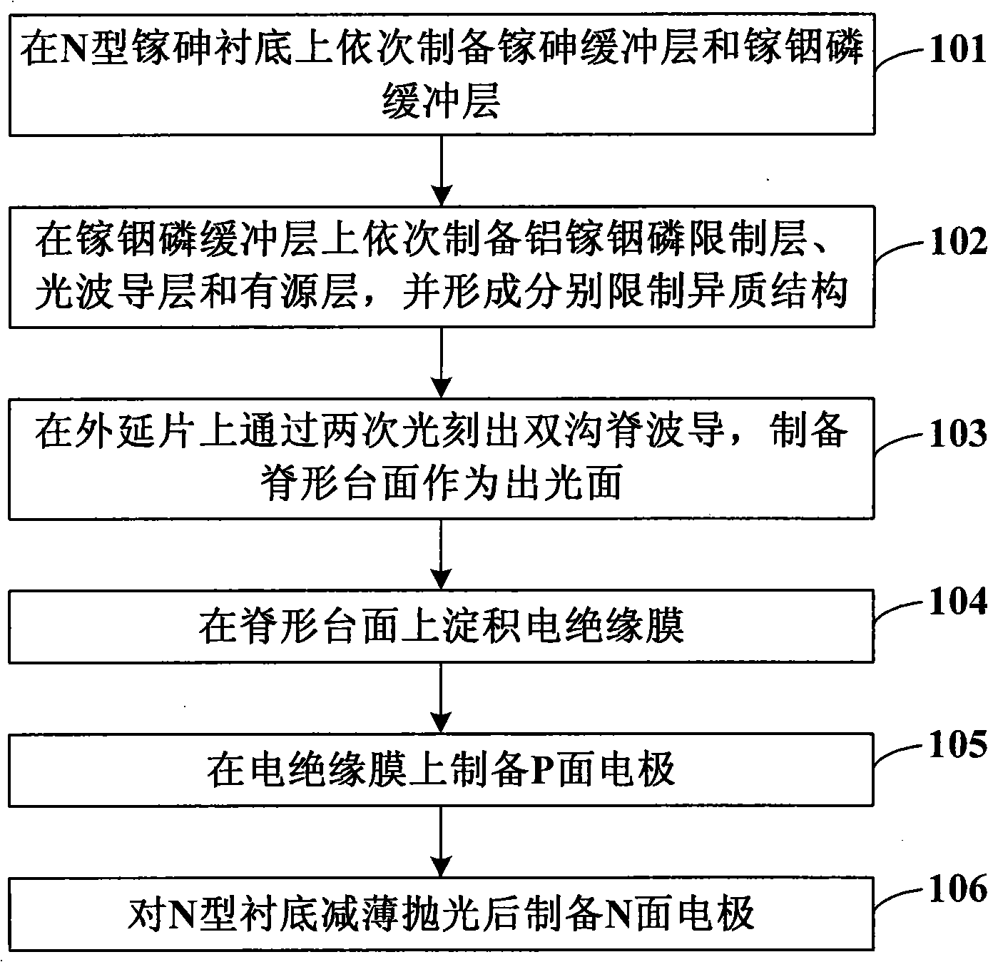
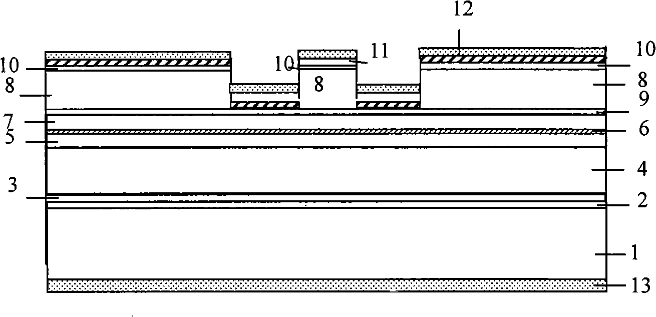
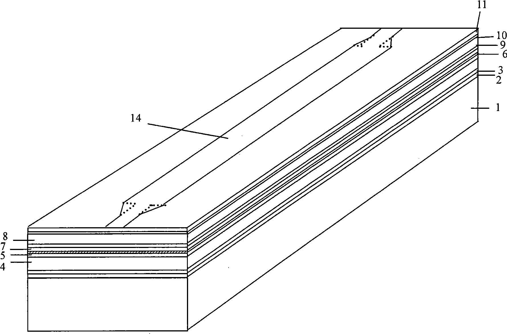
[0059] see Figure 2 to Figure 5 , the method for making quantum well edge-emitting semiconductor laser provided by the invention, the concrete structure of its device and preparation process comprise the following steps:

[0060] (1) Select an N-type GaAs substrate 1 at a temperature of 15 degrees, and epitaxially grow an N-type GaAs buffer layer 2 and an N-type GaInP buffer layer 3 on the N-type GaAs substrate 1 by metal-organic compound vapor deposition method.

[0061] (2) On the N-type GaInP buffer layer 3, epitaxially grow an N-type AlGaInP lower confinement layer 4 with a high aluminum composition, an AlGaInP lower optical waveguide layer 5 with a low aluminum composition, and an active region in sequence 6. Aluminum gallium indium phosphorus upper optical waveguide layer with low aluminum composition 7, P-type aluminum gallium indium phosphorus upper confinement layer with high aluminum composition 8, a thin layer of heavily doped gallium indium phosphorus corrosion st...


PUM


Abstract

The invention discloses a preparation method of a quantum well emitting semiconductor laser used for improving the output light spot, relating to the technical field of a semiconductor laser. The preparation method comprises the steps as follows: A. a Ga-As damping layer and a Ga-In-P damping layer are sequentially prepared on an N-typed Ga-As underlay; B. an Al-Ga-In-P limiting layer, a fibre waveguide layer and an active layer are sequentially prepared on the Ga-In-P damping layer and a structure which limits heterostructures is respectively formed; C. a dual-ridge waveguide is formed on an external extension sheet by etching twice; a ridge-shaped table is prepared to be taken as a light outlet surface; D. an electric insulation film is deposited on the ridge-shaped table; E. a P-surface electrode is prepared on the electric insulation film; F. an N-surface electrode is prepared after the N-typed underlay is thinned and polished. The preparation method of the invention ensures that the original output power and the photoelectric conversion efficiency of the ridge-shaped fibre wave guide laser are not affected basically, increases the parallel divergence angle and improves the output light spot of the laser.

Description

technical field [0001] The invention relates to the technical field of semiconductor lasers, in particular to a method for manufacturing a quantum well edge-emitting semiconductor laser for improving output light spots. Background technique [0002] Semiconductor lasers are widely used in optical storage, optical display, optical communication and other fields due to their advantages such as small size, long life, and high electro-optical conversion efficiency. A large proportion of semiconductor lasers are edge-emitting lasers, which directly use the natural cleavage plane of semiconductor materials as the resonator plane, with simple process and perfect crystal plane. However, some inherent defects of edge-emitting lasers, such as the existence of problems such as large beam divergence angle and poor beam quality, have brought great difficulties to practical applications. [0003] It is well known that the output spot of an edge-emitting quantum well semiconductor laser i...

Claims


Application Information

Patent Timeline
Patent Type & Authority Applications(China)
IPC IPC(8): H01S5/343H01S5/20H01S5/22H01S5/24
Inventor 徐云陈良惠李玉璋曹青宋国峰郭良
Owner INST OF SEMICONDUCTORS - CHINESE ACAD OF SCI
Why Eureka
Try Eureka