Hole injection layer of organic small molecular and electroluminescent device thereof

A technology of electroluminescent devices and hole injection layers, which is applied in the direction of electric solid devices, electrical components, semiconductor devices, etc., can solve the problems of high requirements for equipment and environment, difficult to accurately control the doping ratio, and low yield. Achieve low requirements for equipment and environment, realize large-area preparation, and meet the effect of commercial use

Inactive Publication Date: 2009-01-07
XI AN JIAOTONG UNIV
View PDF0 Cites 15 Cited by
  • Summary
  • Abstract
  • Description
  • Claims
  • Application Information

AI Technical Summary

Problems solved by technology

[0004] However, the P-type doped organic small molecule hole injection layer, the dye-doped organic small molecule hole injection layer and the mixed organic small molecule hole injection transport layer of these P-I-N structure devices with excellent performance are co-evaporated with high vacuum. The method is realized, and the process is more complicated
A general doped hole transport layer requires at least two evaporation sources to work at the same time, and each evaporation source needs to precisely control its evaporation temperature to achieve a certain proportion of doping. In actual production operations, if two materials Or a slight fluctuation in the evaporation temperature of a variety of materials will affect their evaporation rate, resulting in an imbalance in the doping ratio, thereby affecting the performance of the prepared device
It is difficult to accurately control the doping ratio, which is an important shortcoming and deficiency of the doped hole transport layer prepared by high vacuum evaporation, and the requirements for equipment and environment are high, energy consumption is time-consuming, the yield is low, and the corresponding device cost also higher
In addition, it is difficult to achieve large-area uniform deposition by high-vacuum evaporation to prepare a doped hole-transport layer, which is inconsistent with organic electroluminescent devices to large-screen display devices.

Method used


Image

  • Hole injection layer of organic small molecular and electroluminescent device thereof
  • Hole injection layer of organic small molecular and electroluminescent device thereof
  • Hole injection layer of organic small molecular and electroluminescent device thereof

Examples


preparation example Construction

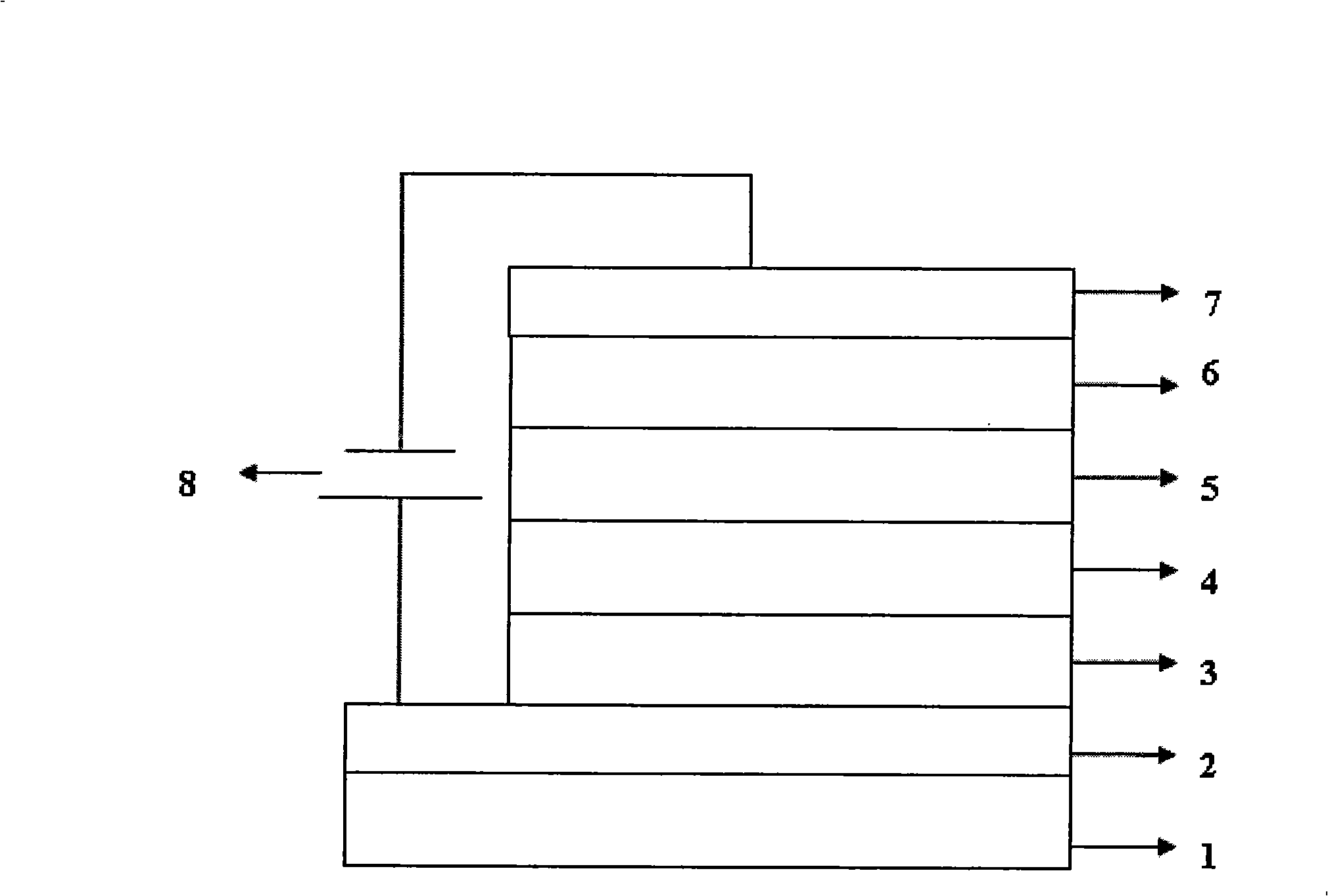
[0036] (3) Preparation of each organic functional layer: Put the spin-coated and dried substrate 1 into a vacuum chamber, and sequentially deposit a layer of hole transport material to form the hole transport layer 4. The transport materials are diamine compounds and triphenylamine compounds, preferably NPB or TPD, the evaporation rate of the material film is 0.01~0.5nm / s, and the film thickness is 10~80nm; a layer is deposited on the hole transport material The organic light-emitting material forms the organic light-emitting layer 5. The organic light-emitting material is one of metal organic complexes, aromatic fused ring compounds, phenanthroline compounds or carbazole derivatives, as well as various fluorescent dyes and phosphorescent dopants. For the miscellaneous light-emitting layer, the evaporation rate of the material film is 0.01-0.5nm / s, and the film thickness is 20-80nm; a layer of electron transport material is evaporated on the organic light-emitting material to form...

Embodiment 1

[0039] Reference now figure 1 The electroluminescent device according to the first embodiment of the present invention has the following structure:

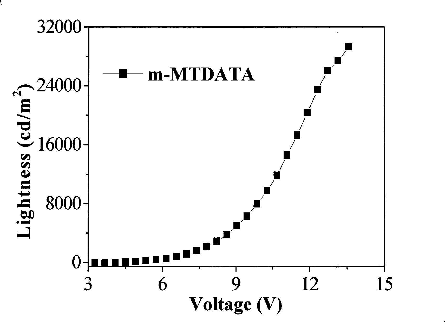
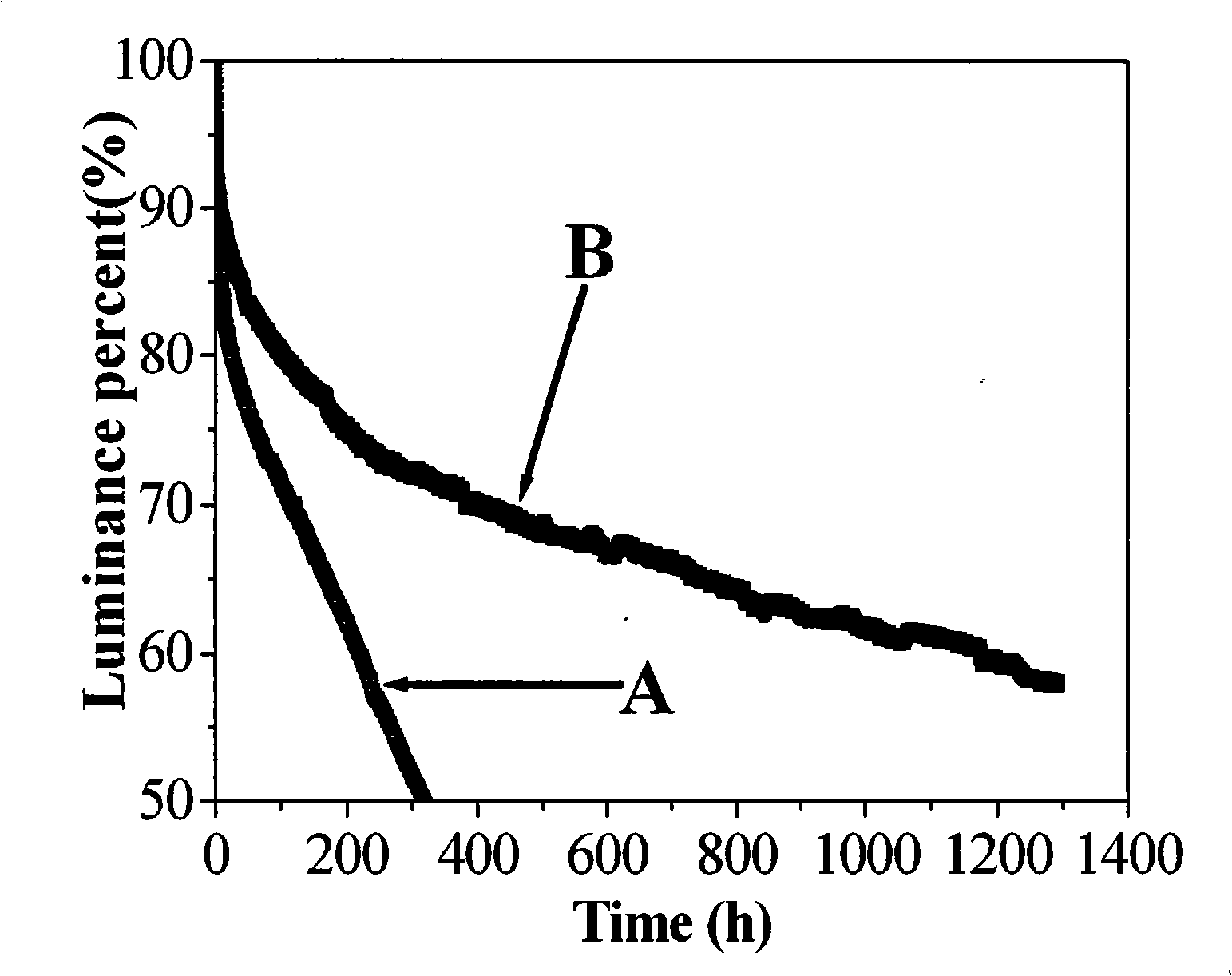
[0040] Glass (plastic) substrate / ITO(100nm) / m-MTDATA(50nm) / NPB(10nm) / Alq 3 (60nm) / LiF(0.5nm) / Al(80nm)

[0041] (1) Cleaning the glass substrate with ITO pre-engraved: Use hot detergent ultrasonic and deionized water ultrasonic method to clean the transparent conductive substrate ITO glass, after cleaning, place it under an infrared lamp to dry, where the conductive The ITO film on the substrate is used as the anode layer of the device. The sheet resistance of the ITO film is 5Ω~100Ω, and the film thickness is 80~280nm. Figure 8(a) is the surface topography of ITOAFM;

[0042] (2) Organic small molecule hole injection layer: Place the above-mentioned cleaned and dried ITO glass on the KW-4A homogenizer, and spin-coat the configured 15mg / ml m-MTDATA chlorobenzene solution by static batching method For the film, the speed of the homoge...

Embodiment 2

[0049] Reference now figure 1 The electroluminescent device according to the second embodiment of the present invention has the following structure:

[0050] Glass (plastic) substrate / ITO(100nm) / NPB: m-MTDATA(50nm) / NPB(10nm) / Alq 3 (60nm) / LiF(0.5nm) / Al(80nm)

[0051] (1) Cleaning of the glass substrate pre-engraved with ITO: Refer to the corresponding process in Example 1;

[0052] (2) Mixed organic small molecule hole injection layer: The mass ratio of NPB to m-MTDATA is 1:3, the concentration of the mixed solution is controlled at 15mg / ml, the solvent is preferably chlorobenzene, and the spin coating and drying conditions refer to the corresponding process in Example 1. Figure 8(d) is an AFM image of the surface morphology of the spin-coated organic small molecule hole injection layer.

[0053] (3) Preparation of each organic functional layer: refer to the corresponding process in Example 1;

[0054] (4) Preparation of the cathode: refer to the corresponding process in Example 1...


PUM


Abstract

The invention discloses an organic micromolecular hole injection layer prepared by using a solution method. An organic film with 10-200nm of thickness is made from an organic micromolecular hole injection material and the mixed solution of the organic micromolecular hole injection material and other organic functional materials by a wet-process film forming process. The invention also discloses an electroluminescent device of the organic micromolecular hole injection layer prepared by using the solution method. The electroluminescent device sequentially comprises a substrate, a transparent anode, an organic micromolecular hole injection layer, a hole transport layer, an organic luminescent layer, an electron transport layer, an electron injection layer and a cathode. Compared with the electroluminescent device of the micromolecular hole transport layer prepared by using a conventional vacuum deposition method, the organic micromolecular injection electroluminescent device causes the service life of the electroluminescent device to increase more than 10 times, which can absolutely meet the commercial application requirement of the device.

Description

Technical field [0001] The invention belongs to the technical field of organic electroluminescence, and relates to an organic small molecule hole injection layer and an electroluminescence device thereof, in particular to an organic small molecule hole injection layer prepared by a solution film forming process and an organic small molecule hole injection layer. Electroluminescent device with molecular hole injection layer. Background technique [0002] The organic electroluminescence device was first reported by C.W. Tang et al. of Kodak in 1987 with a double-layer device structure (Appl. Phys. Lett., 51, 913, (1987)). Because organic electroluminescent devices have the advantages of active light emission, low-voltage direct current drive, full curing, wide viewing angle, low power, fast response speed, and low cost, they have broad application prospects. After nearly two decades of development, rapid development has been achieved in material development and device structure imp...

Claims


Application Information

Patent Timeline
Patent Type & Authority Applications(China)
IPC IPC(8): H01L51/54H01L51/52H01L51/56H01L51/50
Inventor 吴朝新张新稳侯洵
Owner XI AN JIAOTONG UNIV
Why Eureka
Try Eureka