
Flexible high-pass cell electric amalgamation microelectrode array chip apparatus

A microelectrode array and array chip technology, which is applied in the field of chips providing cell electrofusion and devices for biological cell electrofusion, can solve the problem of corrosion resistance, less consideration of antioxidation ability, influence on cell screening, separation and culture, electric field strength and weak electric field gradient, to achieve good fusion effect, high-throughput precise electrofusion control capability, and the effect of improving flux

Inactive Publication Date: 2009-01-14
CHONGQING UNIV
View PDF3 Cites 10 Cited by
  • Summary
  • Abstract
  • Description
  • Claims
  • Application Information

AI Technical Summary

Problems solved by technology

However, the above-mentioned patents generally have a small number of microelectrodes, which cannot achieve high-throughput fusion. On the other hand, the electric field strength and electric field gradient generated by the microelectrodes are relatively weak, which is relatively weak in terms of precise control of cells.
Chinese patent 200610054121.x proposes a cell fusion device based on the chip concept, which solves the problem of high-throughput fusion to a certain extent. , Oxidation disadvantages, in addition, the packaging brought by the silicon substrate chip is more inconvenient, the chip system is not conducive to the sample injection and sample output of cells, which in turn affects the later work of cell screening, separation and cultivation, etc.

Method used


Image

  • Flexible high-pass cell electric amalgamation microelectrode array chip apparatus
  • Flexible high-pass cell electric amalgamation microelectrode array chip apparatus
  • Flexible high-pass cell electric amalgamation microelectrode array chip apparatus

Examples


Embodiment Construction

[0035] The structure of the present invention is described in detail below in conjunction with accompanying drawing:

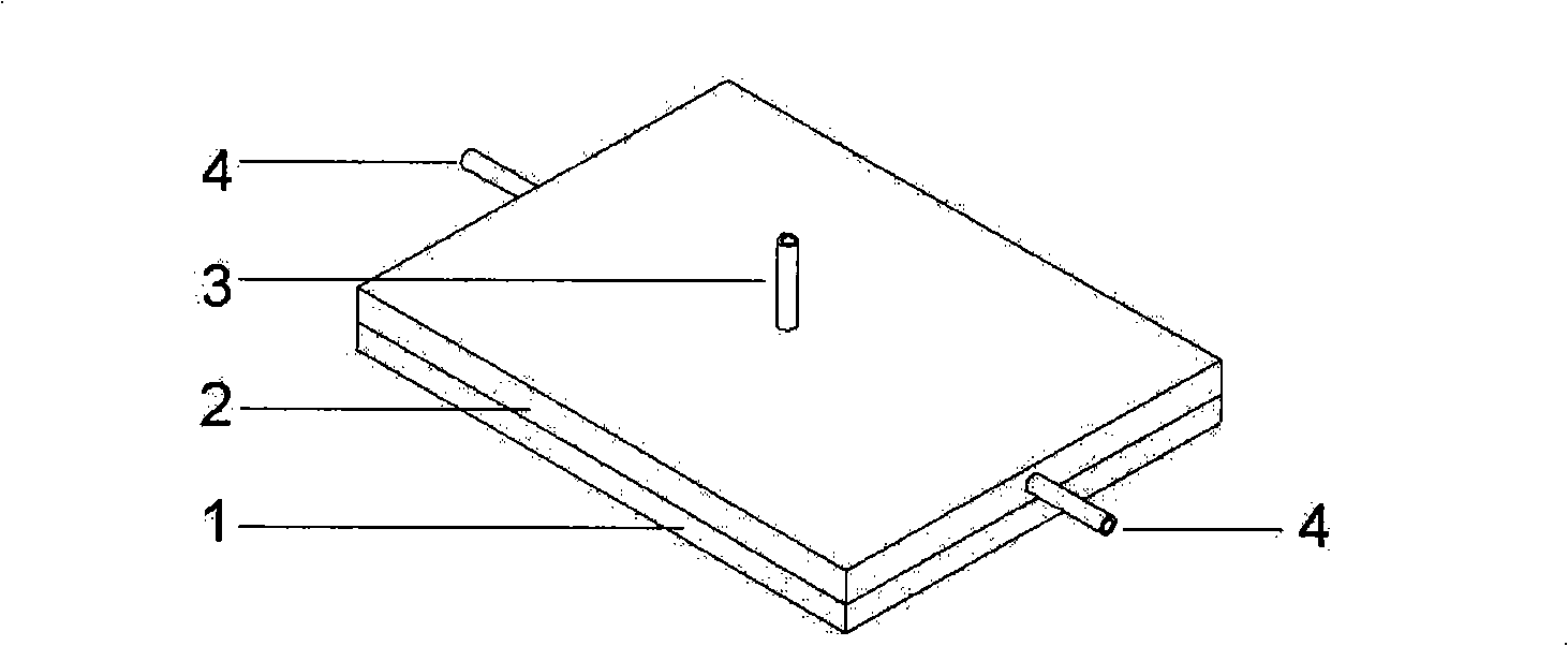
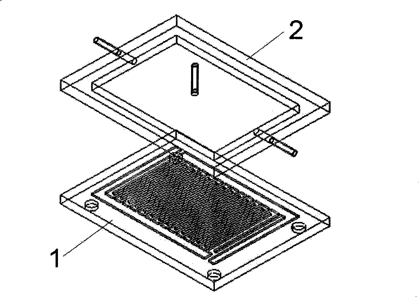
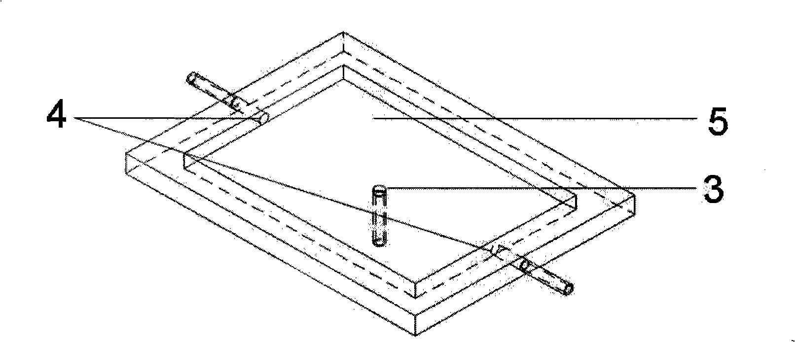
[0036] see figure 1 , figure 2 , image 3 As shown in Fig. 4, the fusion pool 2 is made of hard transparent materials such as glass or plexiglass, and a fusion pool is formed by processing a rectangular groove 5 with a fixed depth in the central area of ​​the sheet-shaped hard transparent material. Weld the wires on the pads 8 of the flexible high-throughput electrofusion cell electrofusion microelectrode array chip 1 (Figure 4B), and then buckle them upside down on the fusion pool 2. The interdigitated array microelectrodes 9 are aligned with the central rectangular recess. Corresponding to the groove 5, an adhesive is used for bonding to form a closed cavity. In the experiment, the flexible high-throughput cell electrofusion microelectrode array chip device was reversed to form a situation in which the flexible high-throughput cell electrofusion microele...


PUM


Abstract

The invention provides a flexible high-flux cell electric fusion microelectrode array chip device, which is composed of an array chip and a fusion pool. The array chip takes a flexible transparent polyimide film as a substrate, the lower surface forms a cross comb-shaped array multimicroelectrode through etching, the electrode group is composed of two comb-shaped microelectrode array electrodes which are mutually crossed but not contacted or connected in electrical structure, and a microchannel between both internal electrodes of the electrode group serves as a service passage; the array chipis inversely buckled on the fusion pool, and the cross comb-shaped array multimicroelectrode on the array chip corresponds to the cell electric fusion pool and falls in the cell electric fusion pool.The invention has the advantages that the use is convenient, the processing method is simple, the cost is extremely inexpensive, and the chip device can not cause damages to operators or cells, thereby being suitable for being widely applied in the fields of genetics, animal and plant distant hybridization breeding, developmental biology, medicine screen, mono-clonal antibody preparing and mammalian clone.

Description

technical field [0001] The invention relates to a device for electrical fusion of biological cells. Specifically, the present invention relates to a chip for providing cell electrofusion, providing and generating the electric field intensity and electric field gradient required for cell alignment, electroporation, and fusion. The patent of the invention relates to the precise control of cells in cell electrofusion and the high-efficiency fusion of cells, and is applicable to genetics, animal and plant distant hybridization breeding, developmental biology, drug screening, monoclonal antibody preparation, mammalian cloning and other fields. Background technique [0002] Biological cells can form new cells through fusion, which is of great significance in the basic field of modern biomedical engineering. Cell fusion technology has gone through several stages of development such as biological, chemical and physical induction. In the 1980s, with the development of electronic in...

Claims


Application Information

Patent Timeline
IPC IPC(8): C12M1/42
CPCC12M35/02C12M23/20C12M23/22C12M23/26C12M25/02
Inventor 杨军胡宁郑小林侯文生廖彦剑曹毅夏斌
Owner CHONGQING UNIV
Learn More