

Method for growing AlN and AlGaN on InAlN buffer layer
A buffer layer and regrowth technology, applied in sustainable manufacturing/processing, electrical components, climate sustainability, etc., can solve the problems of difficult to grasp growth conditions, narrow material growth window, and poor growth repeatability. The effect of improving the flatness of the interface, improving the crystal quality, and improving the level of weapons and equipment
- Summary
- Abstract
- Description
- Claims
- Application Information
AI Technical Summary
Problems solved by technology
Method used
Image

Examples
Embodiment Construction
[0012] What the growth equipment of the present invention used is metal-organic chemical vapor deposition (MOCVD) epitaxial growth system, and the used substrate of material growth is sapphire, Si, SiC etc., and its growth atmosphere is trimethylgallium (TMGa), trimethylaluminum (TMAl ), trimethylindium (TMIn) and ammonia (NH3) as sources of Ga, Al, In and N respectively, with nitrogen, hydrogen or nitrogen-hydrogen mixture as carrier gas.
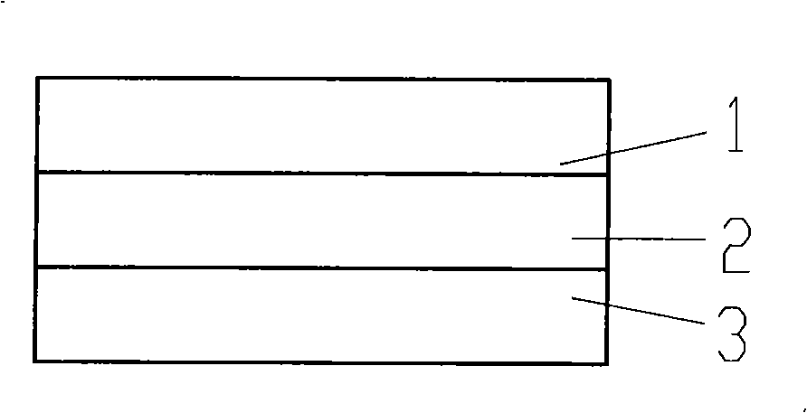
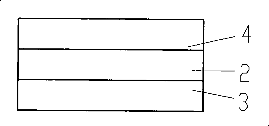
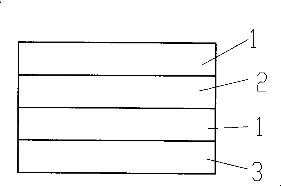
[0013] Below is Figure 1-6 Growth steps and structural conditions of each structure shown: Among them, the growth methods of the InAlN buffer layer, the AlN layer and the AlGaN layer all adopt conventional growth methods. exist Figure 1-6 Among them, 1 is the AlN layer, 2 is the InAlN buffer layer, 3 is the substrate, and 4 is the AlGaN layer.
[0014] figure 1 In order to grow a layer of InAlN buffer layer 2 on the substrate 3, and then grow the AlN layer 1, this layer of AlN can be grown by first growing a low-temperature AlN layer ...
PUM
 Abstract
Description
Claims
Application Information